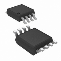
LM3478MM/NOPB National Semiconductor, LM3478MM/NOPB Datasheet - Page 10

LM3478MM/NOPB
Manufacturer Part Number
LM3478MM/NOPB
Description
IC CTRLR SW REG N-CH 8MSOP
Manufacturer
National Semiconductor
Type
Step-Up (Boost), Flyback, Sepicr
Datasheet
1.LM3478MMNOPB.pdf
(24 pages)
Specifications of LM3478MM/NOPB
Internal Switch(s)
No
Synchronous Rectifier
No
Number Of Outputs
1
Voltage - Output
Adjustable
Current - Output
1A
Frequency - Switching
100kHz ~ 1MHz
Voltage - Input
2.97 ~ 40 V
Operating Temperature
-40°C ~ 125°C
Mounting Type
Surface Mount
Package / Case
8-MSOP, Micro8™, 8-uMAX, 8-uSOP,
For Use With
LM3478EVAL - BOARD EVALUATION LM3478
Lead Free Status / RoHS Status
Lead free / RoHS Compliant
Power - Output
-
Other names
LM3478MM
LM3478MMTR
LM3478MMTR
Available stocks
Company
Part Number
Manufacturer
Quantity
Price
Part Number:
LM3478MM/NOPB
Manufacturer:
TI/德州仪器
Quantity:
20 000
www.national.com
Functional Block Diagram
Functional Description
The LM3478 uses a fixed frequency, Pulse Width Modulated
(PWM) current mode control architecture. The block diagram
above shows the basic functionality. In a typical application
circuit, the peak current through the external MOSFET is
sensed through an external sense resistor. The voltage
across this resistor is fed into the Isen pin. This voltage is fed
into the positive input of the PWM comparator. The output
voltage is also sensed through an external feedback resistor
divider network and fed into the error amplifier negative input
(feedback pin, FB). The output of the error amplifier (COMP
pin) is added to the slope compensation ramp and fed into the
negative input of the PWM comparator. At the start of any
switching cycle, the oscillator sets the RS latch using the
switch logic block. This forces a high signal on the DR pin
(gate of the external MOSFET) and the external MOSFET
turns on. When the voltage on the positive input of the PWM
comparator exceeds the negative input, the RS latch is reset
and the external MOSFET turns off.
The voltage sensed across the sense resistor generally con-
tains spurious noise spikes, as shown in Figure 2. These
spikes can force the PWM comparator to reset the RS latch
prematurely. To prevent these spikes from resetting the latch,
a blank-out circuit inside the IC prevents the PWM comparator
from resetting the latch for a short duration after the latch is
set. This duration is about 325ns and is called the blanking
interval and is specified as minimum on-time in the Electrical
Characteristics section. Under extremely light-load or no-load
conditions, the energy delivered to the output capacitor when
10
the external MOSFET in on during the blanking interval is
more than what is delivered to the load. An over-voltage com-
parator inside the LM3478 prevents the output voltage from
rising under these conditions. The over-voltage comparator
senses the feedback (FB pin) voltage and resets the RS latch.
The latch remains in reset state until the output decays to the
nominal value.
OVER VOLTAGE PROTECTION
The LM3478 has over voltage protection (OVP) for the output
voltage. OVP is sensed at the feedback pin (pin 3). If at any-
time the voltage at the feedback pin rises to V
is triggered. See ELECTRICAL CHARACTERISTICS section
for limits on V
OVP will cause the drive pin to go low, forcing the power
MOSFET off. With the MOSFET off, the output voltage will
drop. The LM3478 will begin switching again when the feed-
back voltage reaches V
ELECTRICAL CHARACTERISTICS for limits on V
OVP can be triggered if the unregulated input voltage crosses
7.2V, the output voltage will react as shown in Figure 1. The
internal bias of the LM3478 comes from either the internal
LDO as shown in the block diagram or the voltage at the Vin
pin is used directly. At Vin voltages lower than 7.2V the inter-
nal IC bias is the Vin voltage and at voltages above 7.2V the
internal LDO of the LM3478 provides the bias. At the
switchover threshold at 7.2V a sudden small change in bias
voltage is seen by all the internal blocks of the LM3478. The
control voltage shifts because of the bias change, the PWM
comparator tries to keep regulation. To the PWM comparator,
FB
and V
OVP
.
FB
+ (V
OVP
- V
FB
OVP(HYS)
+ V
OVP(HYS)
OVP
10135506
). See
, OVP
.


