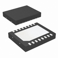
LM3370SD-3021/NOPB National Semiconductor, LM3370SD-3021/NOPB Datasheet - Page 23

LM3370SD-3021/NOPB
Manufacturer Part Number
LM3370SD-3021/NOPB
Description
IC CONV DC/DC DUAL STPDN 16-LLP
Manufacturer
National Semiconductor
Series
PowerWise®r
Type
Step-Down (Buck)r
Datasheet
1.LM3370SD-3021NOPB.pdf
(26 pages)
Specifications of LM3370SD-3021/NOPB
Internal Switch(s)
Yes
Synchronous Rectifier
Yes
Number Of Outputs
2
Voltage - Output
1.2V, 3.3V
Current - Output
600mA
Frequency - Switching
2MHz
Voltage - Input
2.7 ~ 5.5 V
Operating Temperature
-30°C ~ 85°C
Mounting Type
Surface Mount
Package / Case
16-LLP
Power - Output
1.54W
For Use With
LM3370SD-3021EV - BOARD EVALUATION LM3370SD-3021
Lead Free Status / RoHS Status
Lead free / RoHS Compliant
Other names
LM3370SD-3021TR
4.
5.
6.
In mobile phones, for example, a common practice is to place
the DC-DC converter on one corner of the board, arrange the
CMOS digital circuitry around it (since this also generates
noise), and then place sensitive preamplifiers and IF stages
on the diagonally opposing corner. Often, the sensitive cir-
cuitry is shielded with a metal pan and power to it is post-
regulated to reduce conducted noise, using low-dropout
linear regulators.
Micro SMD PACKAGE ASSEMBLY AND USE
Use of the Micro SMD package requires specialized board
layout, precision mounting and careful re-flow techniques, as
detailed in National Semiconductor Application Note 1112.
copper fill as a pseudo-ground plane. Then, connect this
to the ground-plane (if one is used) with several vias. This
reduces ground-plane noise by preventing the switching
currents from circulating through the ground plane. It also
reduces ground bounce at the LM3370 by giving it a low-
impedance ground connection.
Use wide traces between the power components and for
power connections to the DC-DC converter circuit. This
reduces voltage errors caused by resistive losses across
the traces.
Route noise sensitive traces, such as the voltage
feedback path, away from noisy traces between the
power components. The voltage feedback trace must
remain close to the LM3370 circuit and should be direct
but should be routed opposite to noisy components. This
reduces EMI radiated onto the DC-DC converter’s own
voltage feedback trace.
Place noise sensitive circuitry, such as radio IF blocks,
away from the DC-DC converter, CMOS digital blocks
and other noisy circuitry. Interference with noise-
sensitive circuitry in the system can be reduced through
distance.
23
Refer to the section "Surface Mount Technology (SMD) As-
sembly Considerations". For best results in assembly, align-
ment ordinals on the PC board should be used to facilitate
placement of the device. The pad style used with Micro SMD
package must be the NSMD (non-solder mask defined) type.
This means that the solder-mask opening is larger than the
pad size. This prevents a lip that otherwise forms if the solder-
mask and pad overlap, from holding the device off the surface
of the board and interfering with mounting. See Application
Note 1112 for specific instructions how to do this. The 20-
Bump package used for LM3370TL has 300 micron solder
balls and requires 10.82 mils pads for mounting on the circuit
board. The trace to each pad should enter the pad with a 90°
entry angle to prevent debris from being caught in deep cor-
ners. Initially, the trace to each pad should be 7 mil wide, for
a section approximately 7 mil long or longer, as a thermal re-
lief. Then each trace should neck up or down to its optimal
width. The important criteria is symmetry. This ensures the
solder bumps on the LM3370TL re-flow evenly and that the
device solders level to the board. In particular, special atten-
tion must be paid to the pads for bumps A2/B1 of V
E2/D1 of V
nected to large copper planes, inadequate thermal relief can
result in late or inadequate re-flow of these bumps.
The Micro SMD package is optimized for the smallest possi-
ble size in applications with red or infrared opaque cases.
Because the Micro SMD package lacks the plastic encapsu-
lation characteristic of larger devices, it is vulnerable to light.
Backside metallization and/or epoxy coating, along with front-
side shading by the printed circuit board, reduce this sensi-
tivity. However, the package has exposed die edges. In
particular, Micro SMD devices are sensitive to light, in the red
and infrared range, shining on the package’s exposed die
edges.
OUT2
, because V
IN
and PGND are typically con-
www.national.com
OUT1
, and


