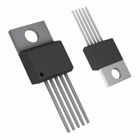
LM2576T-12/NOPB National Semiconductor, LM2576T-12/NOPB Datasheet - Page 18

LM2576T-12/NOPB
Manufacturer Part Number
LM2576T-12/NOPB
Description
IC REG SIMPLE SWITCHER TO-220-5
Manufacturer
National Semiconductor
Series
SIMPLE SWITCHER®r
Type
Step-Down (Buck)r
Specifications of LM2576T-12/NOPB
Internal Switch(s)
Yes
Synchronous Rectifier
No
Number Of Outputs
1
Voltage - Output
12V
Current - Output
3A
Frequency - Switching
52kHz
Voltage - Input
4 ~ 40 V
Operating Temperature
-40°C ~ 125°C
Mounting Type
Through Hole
Package / Case
TO-220-5 (Straight Leads)
Current, Input Bias
50 nA
Current, Output
3 A
Current, Supply
5 mA
Frequency, Oscillator
52 kHz
Package Type
TO-220
Regulator Type
Buck (Step-Down)
Resistance, Thermal, Junction To Case
2 °C/W
Temperature, Operating, Range
-40 to +125 °C
Voltage, Input
40 V
Voltage, Output
12 V
Lead Free Status / RoHS Status
Lead free / RoHS Compliant
Power - Output
-
Lead Free Status / Rohs Status
RoHS Compliant part
Electrostatic Device
Other names
*LM2576T-12
*LM2576T-12/NOPB
LM2576T-12
*LM2576T-12/NOPB
LM2576T-12
Available stocks
Company
Part Number
Manufacturer
Quantity
Price
Company:
Part Number:
LM2576T-12/NOPB
Manufacturer:
TSC
Quantity:
493
Part Number:
LM2576T-12/NOPB
Manufacturer:
NS/国半
Quantity:
20 000
www.national.com
Additional Applications
The switch currents in this buck-boost configuration are
higher than in the standard buck-mode design, thus lowering
the available output current. Also, the start-up input current
of the buck-boost converter is higher than the standard
buck-mode regulator, and this may overload an input power
source with a current limit less than 5A. Using a delayed
turn-on or an undervoltage lockout circuit (described in the
next section) would allow the input voltage to rise to a high
enough level before the switcher would be allowed to turn
on.
Because of the structural differences between the buck and
the buck-boost regulator topologies, the buck regulator de-
sign procedure section can not be used to to select the
inductor or the output capacitor. The recommended range of
inductor values for the buck-boost design is between 68 µH
and 220 µH, and the output capacitor values must be larger
than what is normally required for buck designs. Low input
voltages or high output currents require a large value output
capacitor (in the thousands of micro Farads).
The peak inductor current, which is the same as the peak
switch current, can be calculated from the following formula:
Where f
current operating conditions, the minimum V
the worst case. Select an inductor that is rated for the peak
current anticipated.
Also, the maximum voltage appearing across the regulator is
the absolute sum of the input and output voltage. For a −12V
output, the maximum input voltage for the LM2576 is +28V,
or +48V for the LM2576HV.
The Switchers Made Simple (version 3.0) design software
can be used to determine the feasibility of regulator designs
using different topologies, different input-output parameters,
different components, etc.
NEGATIVE BOOST REGULATOR
Another variation on the buck-boost topology is the negative
boost configuration. The circuit in Figure 11 accepts an input
voltage ranging from −5V to −12V and provides a regulated
−12V output. Input voltages greater than −12V will cause the
output to rise above −12V, but will not damage the regulator.
FIGURE 10. Inverting Buck-Boost Develops −12V
osc
= 52 kHz. Under normal continuous inductor
(Continued)
IN
01147614
represents
18
Typical Load Current
400 mA for V
750 mA for V
Note: Heat sink may be required.
Because of the boosting function of this type of regulator, the
switch current is relatively high, especially at low input volt-
ages. Output load current limitations are a result of the
maximum current rating of the switch. Also, boost regulators
can not provide current limiting load protection in the event of
a shorted load, so some other means (such as a fuse) may
be necessary.
UNDERVOLTAGE LOCKOUT
In some applications it is desirable to keep the regulator off
until the input voltage reaches a certain threshold. An und-
ervoltage lockout circuit which accomplishes this task is
shown in Figure 12, while Figure 13 shows the same circuit
applied to a buck-boost configuration. These circuits keep
the regulator off until the input voltage reaches a predeter-
mined level.
V
Note: Complete circuit not shown.
TH
FIGURE 12. Undervoltage Lockout for Buck Circuit
≈ V
Z1
IN
IN
+ 2V
= −5.2V
= −7V
FIGURE 11. Negative Boost
BE
(Q1)
01147616
01147615


