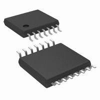
LM25010MH/NOPB National Semiconductor, LM25010MH/NOPB Datasheet - Page 10

LM25010MH/NOPB
Manufacturer Part Number
LM25010MH/NOPB
Description
IC BUCK ADJ 1A 14TSSOP
Manufacturer
National Semiconductor
Type
Step-Down (Buck)r
Specifications of LM25010MH/NOPB
Internal Switch(s)
Yes
Synchronous Rectifier
No
Number Of Outputs
1
Voltage - Output
2.5 ~ 37 V
Current - Output
1A
Frequency - Switching
100kHz ~ 1MHz
Voltage - Input
6 ~ 42 V
Operating Temperature
-40°C ~ 125°C
Mounting Type
Surface Mount
Package / Case
14-TSSOP Exposed Pad, 14-eTSSOP 14-HTSSOP
Dc To Dc Converter Type
Step Down
Pin Count
14
Input Voltage
42V
Output Voltage
2.5 to 37V
Switching Freq
100 to 1000KHz
Output Current
1A
Efficiency
95%
Package Type
TSSOP EP
Output Type
Adjustable
Switching Regulator
Yes
Mounting
Surface Mount
Input Voltage (min)
6V
Operating Temperature Classification
Automotive
Current, Input Bias
1 nA
Current, Output
1 A
Current, Supply
645 μA
Frequency, Oscillator
1 MHz
Regulator Type
Buck (Step-Down), Switching
Resistance, Thermal, Junction To Case
5.2 °C/W
Temperature, Operating, Range
-40 to +125 °C
Voltage, Input
6 to 42 V
Voltage, Output
7 V
For Use With
LM25010EVAL - BOARD EVALUATION LM25010
Lead Free Status / RoHS Status
Lead free / RoHS Compliant
Power - Output
-
Lead Free Status / Rohs Status
Compliant
Other names
*LM25010MH
*LM25010MH/NOPB
LM25010MH
*LM25010MH/NOPB
LM25010MH
Available stocks
Company
Part Number
Manufacturer
Quantity
Price
www.national.com
Over-Voltage Comparator
The feedback voltage at FB is compared to an internal 2.9V
reference. If the voltage at FB rises above 2.9V the on-time
is immediately terminated. This condition can occur if the in-
put voltage, or the output load, changes suddenly. The buck
switch remains off until the voltage at FB falls below 2.5V.
ON-Time Control
The on-time of the internal buck switch is determined by the
R
follows:
The R
by re-arranging Equation 5 to the following:
To set a specific continuous conduction mode switching fre-
quency (Fs), the R
Current Limit
Current limit detection occurs during the off-time by monitor-
ing the recirculating current through the internal current sense
resistor (R
Referring to the Block Diagram, if the current into SGND dur-
ing the off-time exceeds the threshold level the current limit
comparator delays the start of the next on-time period. The
next on-time starts when the current into SGND is below the
threshold and the voltage at FB is below 2.5V. Figure 4 illus-
trates the inductor current waveform during normal operation
and during current limit. The output current I
of the inductor ripple current waveform. The Low Load Cur-
rent waveform illustrates continuous conduction mode oper-
ation with peak and valley inductor currents below the current
limit threshold. When the load current is increased (High Load
Current), the ripple waveform maintains the same amplitude
and frequency since the current falls below the current limit
threshold at the valley of the ripple waveform. Note the aver-
age current in the High Load Current portion of Figure 4 is
above the current limit threshold. Since the current reduces
below the threshold in the normal off-time each cycle, the start
ON
resistor and the input voltage (V
ON
resistor can be determined from the desired on-time
SENSE
). The detection threshold is 1.25A, ±0.25A.
ON
resistor is determined from the following:
IN
), and is calculated as
FIGURE 3. Shutdown Implementation
O
is the average
(5)
(6)
(7)
10
In high frequency applications the minimum value for t
limited by the maximum duty cycle required for regulation and
the minimum off-time of the LM25010 (260 ns, ±15%). The
fixed off-time limits the maximum duty cycle achievable with
a low voltage at VIN. The minimum allowed on-time to regu-
late the desired V
the following:
Shutdown
The LM25010 can be remotely shut down by forcing the RON/
SD pin below 0.7V with a switch or open drain device. See
Figure 3. In the shutdown mode the SS pin is internally
grounded, the on-time one-shot is disabled, the input current
at VIN is reduced, and the V
The V
leasing the RON/SD pin allows normal operation to resume.
The nominal voltage at RON/SD is shown in the Typical Per-
formance Characteristics. When switching the RON/SD pin,
the transition time should be faster than one to two cycles of
the regulator’s nominal switching frequency.
of each on-time is not delayed, and the circuit’s output voltage
is regulated at the correct value. When the load current is fur-
ther increased such that the lower peak would be above the
threshold, the off-time is lengthened to allow the current to
decrease to the threshold before the next on-time begins
(Current Limited portion of Figure 4). Both V
switching frequency are reduced as the circuit operates in a
constant current mode. The load current (I
current limit threshold plus half the ripple current (ΔI/2). The
ripple amplitude (ΔI) is calculated from:
The current limit threshold can be increased by connecting an
external resistor (R
cally is less than 1Ω, and the calculation of its value is ex-
plained in the Applications Information section. If the current
limit threshold is increased by adding R
tinuous load current should not exceed 1.5A, and the peak
current out of the SW pin should not exceed 2A.
CC
regulator is not disabled in the shutdown mode. Re-
20172718
OUT
CL
) between SGND and ISEN. R
at the minimum V
CC
bypass switch is turned off.
CL
IN
, the maximum con-
is determined from
OCL
) is equal to the
OUT
and the
CL
ON
typi-
(8)
(9)
is


