LP3907TL-JJ11/NOPB National Semiconductor, LP3907TL-JJ11/NOPB Datasheet
LP3907TL-JJ11/NOPB
Specifications of LP3907TL-JJ11/NOPB


Related parts for LP3907TL-JJ11/NOPB


LP3907TL-JJ11/NOPB Summary of contents
Page 1
... National Semiconductor Corporation LP3907 Features ■ Compatible with advanced applications processors and FPGAs ■ 2 LDOs for powering Internal processor functions and I/Os ■ ...
Page 2
Typical Application Circuit www.national.com FIGURE 1. Application Circuit 2 30017801 ...
Page 3
FIGURE 2. Application Circuit 3 30017802 www.national.com ...
Page 4
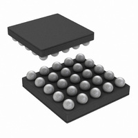
Connection Diagrams and Package Mark Information Note: The physical placement of the package marking will vary from part to part. (*) UZXYTT format: ‘U’ – wafer fab code; ‘Z’ – assembly code; ’XY’ 2 digit date code; ‘TT” – die ...
Page 5
... LP3907TL-JJ11 Voltage “JJ11” LP3907TLX-JJ11 Voltage “JSXS” LP3907TL-JSXS Voltage “JSXS” LP3907TLX-JSXS Voltage “JJCP” LP3907TL-JJCP Voltage “JJCP” LP3907TLX-JJCP Voltage “VXSS” LP3907QTL-VXSS Voltage “VXSS” LP3907QTLX-VXSS Voltage “LNTO” LP3907TL-PLNTO Voltage “LNTO” LP3907TLX-PLNTO Package Type NSC Pkg. Drawing ...
Page 6
Version Default SW1 Voltage JXIP JXQX FX6W JXIX PXPP JXIP JJ11 JJCP JSXS LNTO VXSS JYQX * Voltage is fixed and not programmable. www.national.com Default Voltage Options Default SW2 Voltage 1.2 3.3 1.2 3.3 1 3.3 1.2 3.3 1.5 3.3 ...
Page 7
Order Suffix Spec Version QSQ-JXI7 NOPB QSQ-JXIP NOPB SQ-JXQX NOPB SQ-JXQX S7001874 SQX-JXQX S7001997 SQ-JYQX NOPB SQ-JYQX S7001934 SQX-JYQX S7002030 SQ-PFX6W NOPB SQ-PJXIX NOPB SQ-PXPP NOPB TJXIP NOPB TL-JJ11 NOPB TL-JJCP NOPB TL-JSXS NOPB TL-PLNTO NOPB QTL-VXSS NOPB BJXQX NOPB ...
Page 8
Pin Descriptions LLP Pin micro SMD Name No. pin no. 1 B4, B5 VINLDO12 2 C4 EN_T 3 C3 nPOR 4 C5 GND_SW1 5 D5 SW1 6 E5 VIN1 7 D4 ENSW1 8 E4 FB1 9 D3 GND_C 10 E3 ...
Page 9
... Absolute Maximum Ratings 2) If Military/Aerospace specified devices are required, please contact the National Semiconductor Sales Office/ Distributors for availability and specifications SDA, SCL IN GND to GND SLUG Power Dissipation (P ) D_MAX (T =85°C, T =125° MAX (Note 5) Junction Temperature (T ) J-MAX Storage Temperature Range ...
Page 10
Low Drop Out Regulators, LDO1 and LDO2 Unless otherwise noted 3. 25°C. Limits appearing in boldface type apply over the entire junction temperature range for operation, −40°C to +125°C. 2, Note 7, Note 8, Note 9, ...
Page 11
I/O Electrical Characteristics Unless otherwise noted: Typical values and limits appearing in normal type apply for T type apply over the entire junction temperature range for operation, T Symbol Parameter V Input Low Level IL V Input High Level IH ...
Page 12
Typical Performance Characteristics — LDO Output Voltage Change vs Temperature (LDO1 3.6V 2.6V, 100mA load IN OUT Load Transient (LDO1 – 150mA load IN OUT Line Transient (LDO1) 3.6 - ...
Page 13
Enable Start-up time (LDO1) ) 0-3 2 1mA load IN OUT 30017841 LDO Maximum Load V = 1.74V IN 30017867 Enable Start-up time (LDO2) 0 – load IN ...
Page 14
Typical Performance Characteristics V = 2.8V to 5.5V 25° Shutdown Current vs. Temp Output Voltage vs. Supply Voltage (V = 1.8V) OUT www.national.com — Bucks Output Voltage vs. Supply Voltage 30017843 Output Voltage vs. Supply Voltage ...
Page 15
Typical Performance Characteristics V = 2.8V to 5.5V 25° 1.2V, 2. OUT Efficiency vs Output Current (V =1.2V, L= 2.2µH —(Forced PWM mode) OUT Efficiency vs Output Current (V =1.2V, L= 2.2µH — PWM ...
Page 16
Typical Performance Characteristics V = 4.5V to 5.5V 25° OUT Efficiency vs Output Current ( V =1.8V, L= 2.2µH —Forced PWM mode) OUT Typical Performance Characteristics V = 4.3V to 5.5V 25°C, V ...
Page 17
Typical Performance Characteristics V = 3.6V 25° 1.2V unless otherwise noted IN A OUT Load Transient Response V = 1.2V 300–500mA (PWM Mode) OUT LOAD Line Transient Response V = 3.6 – 4.2V, V ...
Page 18
Start up into PFM Mode V = 1.2V, 30mA load OUT www.national.com Start up into PFM Mode V OUT 30017862 18 = 3.3V, 30mA load 30017880 ...
Page 19
DC/DC Converters OVERVIEW The LP3907 supplies the various power needs of the appli- cation by means of two Linear Low Drop Regulators (LDO1 Supply Load LDO1 analog LDO2 analog SW1 digital SW2 digital *For default values of the regulators, please ...
Page 20
SW1, SW2: Synchronous Step- Down Magnetic DC/DC Converters FUNCTIONAL DESCRIPTION The LP3907 incorporates two high-efficiency synchronous switching buck regulators, SW1 and SW2, that deliver a con- stant voltage from a single Li-Ion battery to the portable system processors. Using a ...
Page 21
When the output drops below the ‘low’ PFM threshold, the cycle repeats to restore the output voltage to ~1.6% above the nominal PWM output voltage. If the load current should increase during PFM mode (see figure below) causing the ...
Page 22
FLEXIBLE POWER SEQUENCING OF MULTIPLE POWER SUPPLIES The LP3907 provides several options for power on sequenc- ing. The two bucks can be individually controlled with ENSW1 and ENSW2. The two LDOs can also be individually con- trolled with ENLDO1 and ...
Page 23
LP3907 Default Power-Up Sequence Power-On Timing Specification Symbol t Programmable Delay from EN_T assertion Programmable Delay from EN_T assertion Programmable Delay from EN_T assertion Programmable Delay from EN_T ...
Page 24
LP3907 Default Power-Off Sequence Symbol t Programmable Delay from EN_T deassertion Programmable Delay from EN_T deassertion Programmable Delay from EN_T deassertion Programmable Delay from EN_T deassertion to V ...
Page 25
Flexible Power-On Reset (i.e., Power Good with delay) The LP3907 is equipped with an internal Power-On-Reset (“POR”) circuit which monitors the output voltage levels on bucks 1 and 2. The nPOR is an open drain logic output which The above ...
Page 26
The above timing diagram details the Power good with delay with respect to the enable signals EN1, and EN2. The RDY1, RDY2 are internal signals derived from the output of two com- parators. Each comparator has been trimmed as follows: ...
Page 27
If the EN1 and RDY1 are initiated in normal operation, then nPOR is asserted and deasserted as explained above. In Case 1, we see that case where EN2 and RDY2 are initi- ated after triggered programmable delay. To prevent the ...
Page 28
Design Implementation of the Flexible Power-On Reset An internal Power-on reset of the IC is used with EN1, and EN2 to produce a reset signal (LOW) to the delay timer nPOR. EN1 and RDY1 or EN2 and RDY2 are used ...
Page 29
Compatible Serial Interface SIGNALS The LP3907 features compatible serial interface, using two dedicated pins: SCL and SDA for I 2 spectively. Both signals need a pull-up resistor according to the ...
Page 30
TRANSFERRING DATA Every byte put on the SDA line must be eight bits long, with the most significant bit (MSB) being transferred first. Each byte of data has to be followed by an acknowledge bit. The acknowledged related clock pulse ...
Page 31
LP3907 Control Registers Register Register Read/ Address Name Write 0x02 ICRA R 0x07 SCR1 R/W 0x10 BKLDOEN R/W 0x11 BKLDOSR R 0x20 VCCR R/W 0x23 B1TV1 R/W 0x24 B1TV2 R/W 0x25 B1RC R/W 0x29 B2TV1 R/W 0x2A B2TV2 R/W 0x2B ...
Page 32
EN_DLY PRESET DELAY SEQUENCE AFTER EN_T ASSERTION EN_DLY<2:0> 000 001 010 011 100 101 110 111 BUCK AND LDO OUTPUT VOLTAGE ENABLE REGISTER (BKLDOEN) – 0X10 This register controls the enables for the Bucks and LDOs — Name ...
Page 33
BUCK1 TARGET VOLTAGE 1 REGISTER (B1TV1) – 0X23 This register allows the user to program the output target volt- age of Buck1. D7-5 — Name BK1_VOUT1 — Access Data Reserved Buck1 Output Voltage (V) 5’h00 5’h01 5’h02 5’h03 5’h04 5’h05 ...
Page 34
BUCK1 RAMP CONTROL REGISTER (B1RC) - 0x25 This register allows the user to program the rate of change between the target voltages of Buck1. D7 Name - - - - Access - - - - Data Reserved Reset 0 www.national.com ...
Page 35
BUCK2 TARGET VOLTAGE 1 REGISTER (B2TV1) – 0X29 This register allows the user to program the output target volt- age of Buck2. D7-5 — Name BK2_VOUT1 — Access Data Reserved Buck2 Output Voltage (V) 5’h00 5’h01 5’h02 5’h03 5’h04 5’h05 ...
Page 36
BUCK2 RAMP CONTROL REGISTER (B2RC) - 0x2B This register allows the user to program the rate of change between the target voltages of Buck2. D7 Name - - - - Access - - - - Data Reserved Reset 0 www.national.com ...
Page 37
BUCK FUNCTION REGISTER (BFCR) – 0x38 This register allows the Buck switcher clock frequency to be spread across a wider range, allowing for less Electro-mag- This register also allows dynamic scaling of the nPOR Delay Timing. The LP3907 is equipped ...
Page 38
LDO1 CONTROL REGISTER (LDO1VCR) – 0X39 This register allows the user to program the output target volt- age of LDO 1. For “JJ11” voltage options LDO1 has a fixed output voltage of 2.85V. D7-5 — Name — Access Data Reserved ...
Page 39
Application Notes ANALOG POWER SIGNAL ROUTING All power inputs should be tied to the main VDD source (i.e. battery), unless the user wishes to power it from another source. (i.e. external LDO output). The analog VDD inputs power the internal ...
Page 40
Graph Showing a Typical Variation in Capacitance vs. DC Bias As shown in the graph, increasing the DC Bias condition can result in the capacitance value that falls below the minimum value given in the recommended capacitor specifications ta- ble. ...
Page 41
Capacitor Min Value C 0.47 LDO1 C 0.47 LDO2 C 10.0 SW1 C 10.0 SW2 Pullup Resistor Both SDA and SCL terminals need to have pullup resistors connected to VINLDO12 or to the power supply of the ...
Page 42
Thermal Performance of the LLP Package The LP3907 is a monolithic device with integrated power FETs. For that reason important to pay special attention to the thermal impedance of the LLP package and to the PCB layout rules ...
Page 43
Physical Dimensions inches (millimeters) unless otherwise noted For ordering, refer to Ordering Information table 0.8 mm 24-Pin LLP Package NS Package SQA24A 43 www.national.com ...
Page 44
X 2.5 mm 25-Bump micro SMD Package NS Package TLA25AAA For ordering, refer to Ordering Information table X1 = 2492 ± 30µ 2492 ± 30µ 600 ± 75µm 44 ...
Page 45
Notes 45 www.national.com ...
Page 46
... For more National Semiconductor product information and proven design tools, visit the following Web sites at: www.national.com Products Amplifiers www.national.com/amplifiers Audio www.national.com/audio Clock and Timing www.national.com/timing Data Converters www.national.com/adc Interface www.national.com/interface LVDS www.national.com/lvds Power Management www.national.com/power Switching Regulators www.national.com/switchers LDOs www.national.com/ldo LED Lighting www ...