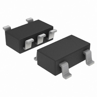
NCP1521BSNT1G ON Semiconductor, NCP1521BSNT1G Datasheet - Page 9

NCP1521BSNT1G
Manufacturer Part Number
NCP1521BSNT1G
Description
IC CONV DC-DC STEPDOWN SOT23-5
Manufacturer
ON Semiconductor
Type
Step-Down (Buck)r
Datasheet
1.NCP1521BSNT1G.pdf
(14 pages)
Specifications of NCP1521BSNT1G
Internal Switch(s)
Yes
Synchronous Rectifier
Yes
Number Of Outputs
1
Voltage - Output
0.9 ~ 3.9 V
Current - Output
600mA
Frequency - Switching
1.5MHz
Voltage - Input
2.7 ~ 5.5 V
Operating Temperature
-40°C ~ 85°C
Mounting Type
Surface Mount
Package / Case
TSOT-23-5, TSOT-5, TSOP-5
Mounting Style
SMD/SMT
Duty Cycle (max)
100 %
Efficiency
90 %
Input / Supply Voltage (max)
3.9 V
Output Current
600 mA
Output Voltage
3.3 V
Switching Frequency
1.5 MHz
Lead Free Status / RoHS Status
Lead free / RoHS Compliant
Power - Output
-
Lead Free Status / Rohs Status
Lead free / RoHS Compliant
Other names
NCP1521BSNT1GOSTR
Available stocks
Company
Part Number
Manufacturer
Quantity
Price
Company:
Part Number:
NCP1521BSNT1G
Manufacturer:
ON
Quantity:
3 000
Part Number:
NCP1521BSNT1G
Manufacturer:
ON/安森美
Quantity:
20 000
Overview
step−down architecture. Both the main (P−Channel
MOSFET) and synchronous (N−Channel MOSFET)
switches are internal.
or three cell NiMH/NiCd battery to portable devices such
as cell phones and PDA. The output voltage is set by an
external resistor divider. The NCP1521B sources at least
600 mA, depending on external components chosen.
PWM/PFM depending on the current required. In PWM
mode, the device can supply voltage with a tolerance of
"3% and 90% efficiency or better. Lighter load currents
cause the device to automatically switch into PFM mode
for reduced current consumption and extended battery life.
protection, current overload protection, and thermal
shutdown protection. As shown in Figure 1, only six
external components are required. The part uses an internal
reference voltage of 0.6 V. It is recommended to keep the
part in shutdown mode until the input voltage is 2.7 V or
higher.
PWM Operating Mode
regulated by modulating the on−time pulse width of the
main switch Q1 at a fixed frequency of 1.5 MHz. The
switching of the PMOS Q1 is controlled by a flip−flop
driven by the internal oscillator and a comparator that
compares the error signal from an error amplifier with the
sum of the sensed current signal and compensation ramp.
This driver switches ON and OFF the upper side transistor
(Q1) and switches the lower side transistor (Q2) in either
ON state or in current source mode. At the beginning of
each cycle, the main switch Q1 is turned ON while Q2 is
in its current source mode by the rising edge of the internal
oscillator clock. The inductor current ramps up until the
sum of the current sense signal and compensation ramp
becomes higher than the error voltage amplifier. Once this
has occurred, the PWM comparator resets the flip−flop, Q1
is turned OFF and the synchronous switch Q2 is turned in
its ON state. Q2 replaces the external Schottky diode to
reduce the conduction loss and improve the efficiency. To
avoid overall power loss, a certain amount of dead time is
introduced to ensure Q1 is completely turned OFF before
Q2 is being turned ON.
The NCP1521B uses a constant frequency, current mode
It delivers a constant voltage from either a single Li−Ion
The NCP1521B works with two modes of operation;
Additional features include soft−start, undervoltage
In this mode, the output voltage of the NCP1521B is
OPERATION DESCRIPTION
http://onsemi.com
9
PFM Operating Mode
current
consumption. The output regulation is implemented by
pulse frequency modulation. If the output voltage drops
below the threshold of PFM comparator, a new cycle will
be initiated by the PFM comparator to turn on the switch
Q1. Q1 remains ON during the minimum on time of the
structure while Q2 is in its current source mode. The peak
inductor current depends upon the drop between input and
output voltage. After a short dead time delay where Q1 is
switched OFF, Q2 is turned in its ON state. The negative
current detector will detect when the inductor current drops
below zero and sends the signal to turn Q2 to current source
mode to prevent a too large deregulation of the output
voltage. When the output voltage falls below the threshold
of the PFM comparator, a new cycle starts immediately.
Under light load conditions, the NCP1521B enters in low
I
100mA/div
V
10mV/div
V
2V/div
Lx
out
Lx
Figure 28. PFM Mode Switching Waveform
PFM
V
10mV/div
(V
(V
OUT
Figure 27. PWM Switching Waveform
IN
V
2V/div
IN
Lx
= 3.6 V, V
I
100mA/div
= 3.6 V, V
Lx
mode
OUT
OUT
200 ns/div
operation
= 1.2 V, I
= 1.2 V, I
OUT
to
OUT
= 600 mA)
= 0 mA)
reduce
power


