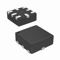
SC195ULTRT Semtech, SC195ULTRT Datasheet

SC195ULTRT
Specifications of SC195ULTRT
Available stocks
Related parts for SC195ULTRT
SC195ULTRT Summary of contents
Page 1
... SC195 a versatile device ideal for step-down regulation in products needing high efficiency and a small PCB footprint. SC195 IN 1.0µ 4.7µF OUT CTL3 CTL2 GND CTL1 CTL0 © 2010 Semtech Corporation SC195 OUT 0.8V to 3.3V C OUT 10µF 1 ...
Page 2
... OUT MLPQ-UT8; 1.5 x 1.5, 8 LEAD θ = 116°C/W JA Marking Information SC195 yw = Date code Ordering Information Device SC195ULTRT SC195EVB Notes (1) Available in tape and reel only. A reel contains 3,000 devices. (2) Lead-free packaging only. Device is WEEE and RoHS compliant and halogen-free GND 5 Table 1 – Output Voltage Settings ...
Page 3
Absolute Maximum Ratings IN ( ...
Page 4
Electrical Characteristics (continued) Parameter Switching Frequency Soft-Start Thermal Shutdown Thermal Shutdown Hysteresis Logic Inputs - CTL0, CTL1, CTL2, and CTL3 Input High Voltage Input Low Voltage Input High Current Input Low Current Notes (1) Maximum output voltage is limited to ...
Page 5
Typical Characteristics V = 4.0V for V = 3.3V 3.6V for all others OUT IN Efficiency vs OUT 100 90 3.3V 2. 0.1 ...
Page 6
Typical Characteristics (continued 4.0V for V = 3.3V 3.6V for all others OUT IN Frequency vs. Temperature 4 3.8 1V 1.8V 3.3V 3.6 2.8V 3.4 3.2 3 -40 - Temperature (°C) ...
Page 7
Typical Characteristics (continued) Light Load Switching — (50mV/div) OUT V (2V/div (200mA/div) LX Time (400ns/div) Light Load Switching — (50mV/div) OUT V (2V/div (200mA/div) LX Time (400ns/div) Heavy Load Switching — V ...
Page 8
Typical Characteristics (continued) Heavy Load Switching — (50mV/div) OUT V (2V/div (200mA/div) LX Time (200ns/div) Heavy Load Soft-start I = 500mA LOAD I (200mA/div (1.0V/div) OUT I (500mA/div) LX Time (40μs/div) Load Transient Response ...
Page 9
Typical Characteristics (continued) Load Transient Response — 200 to 500mA V (100mV/div) OUT I (500mA/div (500mA/div) LOAD Time (20μs/div) VID Transient Response — PSAVE 1.2V to 1.8V transition V (500mV/div) OUT I (200mA/div (2.0V/div) CTL2 Time ...
Page 10
Pin Descriptions Pin Pin Name Pin Function Control bit 2 — see Table 1, page 2, for decoding. This pin has a weak pull-down resistor (> 1MΩ) in place at 1 CTL2 reset that is removed when CTL2 is pulled ...
Page 11
Block Diagram OSC & Slope 500mV Ref 4 CTL3 3 CTL2 Voltage Select 2 CTL1 1 CTL0 5 OUT Plimit Amp Generator PWM Comp Error Amp PSAVE Comp 8 IN Current Amp Control 7 LX Logic Nlimit Amp 6 GND ...
Page 12
Applications Information General Description The SC195 is a synchronous step-down Pulse Width Modulated (PWM) DC-DC regulator utilizing a 3.5MHz fixed-frequency voltage mode architecture. The device is designed to operate in fixed-frequency PWM mode and enter power save (PSAVE) mode utilizing ...
Page 13
Applications Information (continued) SC195 OUT CTL3 CTL2 GND Enable CTL1 CTL0 Figure 1 — Application Circuit with External Resistors To simplify the design recommended to program the output setting to 1.0V, use ...
Page 14
Applications Information (continued) Load Demand (I ) OUT OFF V +2.5% OUT V OUT V -2% OUT BURST V LX PWM Mode at PSAVE Mode at Medium/High Light Load Load Time Figure 2 — Transitions Between PWM and PSAVE Modes ...
Page 15
Applications Information (continued) pole output filter corner frequency defined by the equation where L = 1μH and C = 10μF. OUT When selecting output filter components, the LC product should not vary over a wide range. Selection of smaller inductor ...
Page 16
Applications Information (continued) C Selection OUT The internal voltage loop compensation in the SC195 limits the minimum output capacitor value to 10μF. This is due to its influence on the the loop crossover frequency, phase margin, and gain margin. Increasing ...
Page 17
Applications Information (continued) The input voltage ripple is at maximum level when the input voltage is twice the output voltage (50% duty cycle scenario). The input capacitor provides a low impedance loop for the edges of pulsed current drawn by ...
Page 18
Outline Drawing — MLPQ-UT8 A PIN 1 INDICATOR (LASER MARK) A aaa 0.20 1 0.25 0.17 NOTES: CONTROLLING DIMENSIONS ARE IN MILLIMETERS (ANGLES IN DEGREES DIM ...
Page 19
Land Pattern — MLPQ-UT8 NOTES: 1. CONTROLLING DIMENSIONS ARE IN MILLIMETERS (ANGLES IN DEGREES). 2. THIS LAND PATTERN IS FOR REFERENCE PURPOSES ONLY. CONSULT YOUR MANUFACTURING GROUP TO ENSURE YOUR COMPANY'S MANUFACTURING GUIDELINES ARE MET. ...
Page 20
... SEMTECH PRODUCTS ARE NOT DESIGNED, INTENDED, AUTHORIZED OR WARRANTED TO BE SUITABLE FOR USE IN LIFE- SUPPORT APPLICATIONS, DEVICES OR SYSTEMS OR OTHER CRITICAL APPLICATIONS. INCLUSION OF SEMTECH PRODUCTS IN SUCH APPLICATIONS IS UNDERSTOOD TO BE UNDERTAKEN SOLELY AT THE CUSTOMER’ ...


