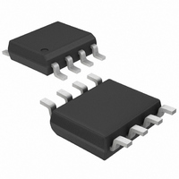
ICL7660ESA+ Maxim Integrated Products, ICL7660ESA+ Datasheet - Page 2

ICL7660ESA+
Manufacturer Part Number
ICL7660ESA+
Description
IC VOLTAGE CONVERTER 8-SOIC
Manufacturer
Maxim Integrated Products
Type
Switched Capacitor (Charge Pump), Divider, Doubler, Invertingr
Specifications of ICL7660ESA+
Internal Switch(s)
Yes
Synchronous Rectifier
No
Number Of Outputs
1
Current - Output
20mA
Frequency - Switching
10kHz
Voltage - Input
1.5 ~ 10 V
Operating Temperature
-40°C ~ 85°C
Mounting Type
Surface Mount
Package / Case
8-SOIC (3.9mm Width)
Power - Output
471mW
Function
Inverting/Step Up
Output Voltage
- 1.5 V to - 10 V or 3 V to 20 V
Output Current
20 mA
Maximum Operating Temperature
+ 85 C
Minimum Operating Temperature
- 40 C
Mounting Style
SMD/SMT
Primary Input Voltage
10V
No. Of Outputs
1
No. Of Pins
8
Operating Temperature Range
-40°C To +85°C
Dropout Voltage Vdo
500mV
Filter Terminals
SMD
Rohs Compliant
Yes
Lead Free Status / RoHS Status
Lead free / RoHS Compliant
Voltage - Output
-
Lead Free Status / Rohs Status
Lead free / RoHS Compliant
± 5V、1Gsps、8ビットADC
2.2GHzトラック/ホールドアンプ内蔵
ABSOLUTE MAXIMUM RATINGS
V
V
V
V
AUXEN1, AUXEN2 to GND .....................-0.3V to (V
V
Between GNDs......................................................-0.3V to +0.3V
V
V
PECL Digital Output Current ...............................................50mA
REFIN to GNDR ........................................-0.3V to (V
REFOUT Current ................................................+100µA to -5mA
ICONST, IPTAT to GNDI .......................................-0.3V to +1.0V
TTL/CMOS Control Inputs (DEMUXEN,
Stresses beyond those listed under “Absolute Maximum Ratings” may cause permanent damage to the device. These are stress ratings only, and functional
operation of the device at these or any other conditions beyond those indicated in the operational sections of the specifications is not implied. Exposure to
absolute maximum rating conditions for extended periods may affect device reliability.
DC ELECTRICAL CHARACTERISTICS
(V
unless otherwise noted. Typical values are at T
2
ACCURACY
ANALOG INPUTS
VOS ADJUST CONTROL INPUT
REFERENCE INPUT AND OUTPUT
CC
CC
CC
CC
EE
CC
CC
Resolution
Integral Nonlinearity (Note 1)
Differential Nonlinearity (Note 1)
Missing Codes
Full-Scale Input Range
Common-Mode Input Range
Input Resistance
Input Resistance Temperature
Coefficient
Input Resistance (Note 2)
Input V
Reference Output Voltage
Reference Output Load
Regulation
Reference Input Resistance
DIVSELECT)..........................................-0.3V to (V
CC
A to GNDA .........................................................-0.3V to +6V
D to GNDD.........................................................-0.3V to +6V
I to GNDI ............................................................-0.3V to +6V
O to GNDD ........................................-0.3V to (V
A to V
A to V
_______________________________________________________________________________________
to GNDI..............................................................-6V to +0.3V
A = V
OS
CC
CC
PARAMETER
CC
Adjust Range
D .......................................................-0.3V to +0.3V
I.........................................................-0.3V to +0.3V
I = V
CC
D = +5.0V ±5%, V
∆REFOUT
SYMBOL
REFOUT
R
R
V
DNL
V
RES
TC
INL
R
FSR
VOS
REF
CM
EE
IN
R
= -5.0V ±5%, V
A
T
T
No missing codes guaranteed
Note 1
Signal + offset w.r.t. GNDI
VIN+ and VIN- to GNDI, T
VOSADJ = 0 to 2.5V
Driving REFIN input only
0 < I
Referenced to GNDR
= +25°C.)
A
A
= +25°C
= +25°C
CC
CC
CC
CC
SOURCE
D + 0.3V)
D + 0.3V)
D + 0.3V)
I + 0.3V)
CC
< 2.5mA
O = +3.0V to V
CONDITIONS
RSTIN+, RSTIN- ......................................-0.3V to (V
VOSADJ Adjust Input ................................-0.3V to (V
CLK+ to CLK- Voltage Difference..........................................±3V
CLK+, CLK-.....................................(V
CLKCOM.........................................(V
VIN+ to VIN- Voltage Difference ............................................±2V
VIN+, VIN- to GNDI................................................................±2V
Continuous Power Dissipation (T
Operating Temperature Range
Operating Junction Temperature.....................................+150°C
Storage Temperature Range .............................-65°C to +150°C
192-Contact ESBGA (derate 61mW/°C above +70°C)......4.88W
(with heatsink and 200 LFM airflow,
derate 106mW/°C above +70°C) ........................................8.48W
MAX104CHC........................................................0°C to +70°C
A
= +25°C
CC
D, REFIN connected to REFOUT, T
2.475
MIN
-0.5
-0.5
475
±4
49
14
8
4
A
= +70°C)
±0.25
±0.25
EE
EE
TYP
±0.8
±5.5
2.50
500
150
50
25
5
- 0.3V) to (GNDD + 1V)
- 0.3V) to (GNDD + 1V)
A
2.525
None
MAX
= T
525
0.5
0.5
51
5
CC
MIN
CC
O + 0.3V)
I + 0.3V)
ppm/°C
to T
UNITS
Codes
mVp-p
LSB
LSB
LSB
Bits
mV
kΩ
kΩ
Ω
V
V
MAX
,


