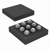
LM3207TL-2.53/NOPB National Semiconductor, LM3207TL-2.53/NOPB Datasheet - Page 3

LM3207TL-2.53/NOPB
Manufacturer Part Number
LM3207TL-2.53/NOPB
Description
IC BUCK SYNC 2.53V .65A 9USMD
Manufacturer
National Semiconductor
Series
PowerWise®r
Type
Step-Down (Buck)r
Datasheet
1.LM3207TLNOPB.pdf
(24 pages)
Specifications of LM3207TL-2.53/NOPB
Internal Switch(s)
Yes
Synchronous Rectifier
Yes
Number Of Outputs
1
Voltage - Output
2.53V
Current - Output
650mA
Frequency - Switching
2MHz
Voltage - Input
2.7 ~ 5.5 V
Operating Temperature
-30°C ~ 85°C
Mounting Type
Surface Mount
Package / Case
9-MicroSMD
For Use With
LM3207TL-2.53EV - BOARD EVAL LM3207 WCDMA/CDMALM3207TLEV - BOARD EVALUATION LM3207TL
Lead Free Status / RoHS Status
Lead free / RoHS Compliant
Power - Output
-
Other names
LM3207TL-2.53TR
LDO
V
V
I
I
I
I
I
I
Switcher
V
V
I
I
R
R
I
F
V
V
I
SC
PUT
PD
PDT
Q_LDO + PWM
PIN,EN
SHDN
Q_PWM
LIM,PFET
PIN,EN
OSC
LDO
LDO,MIN
FB, MIN
FB, MAX
IH,EN
IL,EN
DSON(P)
DSON(N)
Absolute Maximum Ratings
If Military/Aerospace specified devices are required,
please contact the National Semiconductor Sales Office/
Distributors for availability and specifications.
Electrical Characteristics
boldface type apply over the full operating ambient temperature range (−30°C
specifications apply to all LM3207 LDO options with: PV
PV
PGND to SGND
EN, FB, V
SW
PV
Continuous Power Dissipation
(Note 3)
Junction Temperature (T
Symbol
IN
IN
LDO
to SGND
CON
, EN
LDO Output Voltage
Minimum LDO Output Voltage Iout = 10mA, PV
Short circuit current(DC)
Pull-up current (transient)
DC Pull-down current (DC)
Pull-down current (transient)
DC Bias current into PV
LDO Pin pull down current
Feedback Voltage at minimum
setting
Feedback Voltage at maximum
setting
Shutdown supply current
DC bias current into PV
Pin-pin resistance for PFET
Pin-pin resistance for NFET
Switch peak current limit
Internal oscillator frequency
Logic high input threshold
(PWM, LDO)
Logic low input threshold
(PWM, LDO)
PWM Pin pull down current
LDO
, LDO
Parameter
J-MAX
)
IN
IN
Internally Limited
(Notes 2, 6, 7)
to (PV
−0.2V to +6.0V
−0.2V to +0.2V
−0.2V to +0.2V
(SGND −0.2V)
(PGND −0.2V)
to (V
Iout = 0 mA
V
V
(Note 12)
V
V
(Note 12)
V
EN
V
V
EN = EN
(Note 8)
V
EN = 3.6V, No Switching (Note 9)
I
I
(Note 10)
SW
SW
(Notes 1, 2)
LDO
LDO
LDO
LDO
CON
CON
CON
CON
w/6.0V max
w/6.0V max
LDO
= 200mA
= - 200mA
DD
IN
= 0
= V
= PV
= 1.44V, PV
= 2V, FB = 0V, No Switching,
= 0.32V
= 1.44V, PV
= 2V, FB = 0V, EN
+150°C
+0.2V)
+0.2V)
= EN = 3.6V (Note 9)
LDO(nom)
LDO
IN
IN
= V
, EN
= SW = V
Conditions
Limits in standard typeface are for T
IN
IN
/2, PV
LDO
3
= EN
IN
IN
= 3V
= 3V
= 4.2V
= 0
Operating Ratings
Thermal Properties
CON
Storage Temperature Range
Maximum Lead Temperature
Input Voltage Range
Recommended Load Current
Junction Temperature (T
Ambient Temperature (T
(Note 4)
Junction-to-Ambient Thermal
Resistance (θ
(Note 5)
LDO
IN
(Soldering, 10 sec)
LDO
= 3V
= 0V,
= EN = 3.6V.
= 0V ,
≤
T
JA
A
= T
), TLA09 Package
3.537
0.75
Min
-2.6
150
935
1.7
1.2
J
≤
+85°C). Unless otherwise noted, all
A
J
) Range
) Range
1100
0.01
Typ
140
300
-50
1.2
0.8
3.6
1.1
50
5
2
5
A
= T
(Notes 1, 2)
J
= 25°C. Limits in
3.683
1200
Max
+2.6
-200
0.85
200
230
415
485
1.6
1.6
2.3
0.5
10
10
2
−65°C to +150°C
−30°C to +125°C
−30°C to +85°C
0mA to 650mA
2.7V to 5.5V
www.national.com
100°C/W
Units
MHz
+260°C
mΩ
mΩ
mA
mA
mA
mA
mA
mA
mA
uA
µA
µA
%
%
V
V
V
V


