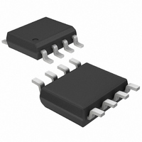
MAX887HESA+ Maxim Integrated Products, MAX887HESA+ Datasheet - Page 11

MAX887HESA+
Manufacturer Part Number
MAX887HESA+
Description
IC DC-DC CONV LN 8-SOIC
Manufacturer
Maxim Integrated Products
Type
Step-Down (Buck)r
Datasheet
1.MAX887HESA.pdf
(12 pages)
Specifications of MAX887HESA+
Internal Switch(s)
Yes
Synchronous Rectifier
Yes
Number Of Outputs
1
Voltage - Output
1.25 ~ 10 V
Current - Output
600mA
Frequency - Switching
300kHz
Voltage - Input
3.5 ~ 11 V
Operating Temperature
-40°C ~ 85°C
Mounting Type
Surface Mount
Package / Case
8-SOIC (3.9mm Width)
Power - Output
471mW
Output Voltage
1.25 V to 10.5 V
Output Current
600 mA
Input Voltage
3.5 V to 11 V
Supply Current
2.7 mA
Switching Frequency
300 KHz
Maximum Operating Temperature
+ 85 C
Minimum Operating Temperature
- 40 C
Lead Free Status / RoHS Status
Lead free / RoHS Compliant
Bypass V+ to GND using a 0.33µF capacitor. Also
bypass VL to GND with a 2.2µF capacitor, and VREF to
GND using a 0.047µF capacitor. These capacitors
should be placed within 0.2in (5mm) of their respective
pins. A small ceramic capacitor (C1) of around 100pF
to 470pF should be added in parallel with R1 to com-
pensate for stray capacitance at the FB pin and output
capacitor ESR.
A 1A external diode (D1) is required as an output recti-
fier to pass inductor current during the second half of
each cycle. This diode operates in PFM mode and dur-
ing transition periods while the synchronous rectifier is
off. Use a Schottky diode to prevent the slow internal
diode of the N-channel MOSFET from turning on.
High switching frequencies and large peak currents
make PC board layout a very important part of design.
Poor design can result in excessive EMI on the feed-
back paths and voltage gradients in the ground plane,
both of which can result in instability or regulation
errors. Power components, such as the MAX887,
inductor, input filter capacitor, and output filter capaci-
tor should be placed as close together as possible,
and their traces kept short, direct, and wide. Connect
their ground pins at a common node in a star-ground
configuration. Keep the extra copper on the board and
integrate into ground as a pseudo-ground plane. The
external voltage-feedback network should be very
close to the FB pin, within 0.2in (5mm). Keep noisy
traces, such as from the LX pin, away from the voltage-
feedback network, and separate using grounded cop-
per. Place the small bypass capacitors (C1, C3, C5,
and C6) within 0.2in (5mm) of their respective pins. The
MAX887 evaluation kit manual illustrates an example
PC board layout, routing, and pseudo-ground plane.
PC Board Layout and Routing
______________________________________________________________________________________
Output Diode Selection
Step-Down, PWM DC-DC Converter
100% Duty Cycle, Low-Noise,
TRANSISTOR COUNT: 2006
SUBSTRATE CONNECTED TO GND
___________________Chip Information
11


