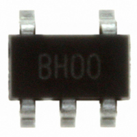
SC4503TSKTRT Semtech, SC4503TSKTRT Datasheet - Page 13

SC4503TSKTRT
Manufacturer Part Number
SC4503TSKTRT
Description
IC SW REG STEP-UP 1.4A TSOT23-5
Manufacturer
Semtech
Type
Step-Up (Boost), Sepicr
Datasheet
1.SC4503TSKTRT.pdf
(22 pages)
Specifications of SC4503TSKTRT
Internal Switch(s)
Yes
Synchronous Rectifier
No
Number Of Outputs
1
Voltage - Output
Adj to 27V
Current - Output
1.4A
Frequency - Switching
1.3MHz
Voltage - Input
2.5 ~ 20 V
Operating Temperature
-40°C ~ 85°C
Mounting Type
Surface Mount
Package / Case
TSOT-23-5, TSOT-5, TSOP-5
Lead Free Status / RoHS Status
Lead free / RoHS Compliant
Power - Output
-
Other names
SC4503TSKTR
Available stocks
Company
Part Number
Manufacturer
Quantity
Price
Company:
Part Number:
SC4503TSKTRT
Manufacturer:
TI
Quantity:
6 000
Part Number:
SC4503TSKTRT
Manufacturer:
SEMTECH/美国升特
Quantity:
20 000
circuit from the driving logic gate during fault condition.
In Figure 5(f) the shutdown pin is driven from a logic gate
whose V
The diode clamps the maximum shutdown pin voltage to
one diode voltage above the input power supply.
During soft-start, C
the R
steady state, the voltage drop across R
down pin voltage according to the following equation:
In order for the SC4503 to achieve its rated switch current,
puts an upper limit on R
voltage applied to R
50µA with
The largest R
If the enable signal is less than 2V, then the interfacing
options shown in Figures 5(d) and 5(e) will be preferred. The
methods shown in Figures 5(a) and 5(c) can still be used
however the switch current limit will be reduced. Variations
of
and temperature are shown in the “Typical Characteristics”.
Shutdown pin current decreases as temperature increases.
Switch current limit at a given
temperature rises. Lower shutdown pin current fl owing
through R
pin voltage. However reduction in switch current limit (at
a given
effect.
Feed-Forward Compensation
Figure 6 shows the equivalent circuit of a boost converter.
Important poles and zeros of the overall loop response
are:
Low frequency integrator pole,
2007 Semtech Corp.
POWER MANAGEMENT
Applications Information (Cont.)
SS
<
<
current and the shutdown pin current,
OH
must be greater than 2V in steady state. This
and switch current limit with
SS
is higher than the supply voltage to the SC4503.
=
=
at high temperature results in higher shutdown
SS
µ
µ
can be found using (14):
−
−
) at high temperature is the dominant
−
−
SS
= =
SS
is charged by the difference between
). The maximum specifi ed
SS
(see “Electrical Characteristics”).
for a given enable voltage V
ω
=
−
SHDN SS
SHDN
SS
also decreases as
reduces the shut-
SS
,
pin voltage
(14)
EN
. In
(=
is
13
Output fi lter pole,
Compensating zero,
Right half plane (RHP) zero,
The poles p
shift in the loop response. For stable operation, the over-
all loop gain should cross 0dB with -20dB/decade slope.
Due to the presence of the RHP zero, the 0dB crossover
frequency should not be more than
compensating zero z
general the converter is more stable with widely spaced
fi lter pole p
low frequency when either the duty-cycle D or the output
current I
and larger output capacitors especially when operating at
high
A feed-forward capacitor C
of C
tor current and the output voltage during load transient.
Starting with a value between
adjusted until there is no excessive ringing or overshoot in
inductor current and output voltage during load transient.
Sizing the inductor such that its ripple current is about 0.5A
also improves phase margin and transient response.
V
V
V
V
IN
IN
IN
IN
COMP
COMP
COMP
COMP
4
Figure 6. Simplifi ed Equivalent Model of a Boost
Figure 6.
Figure 6. Simplifi ed Equivalent Model of a Boost
Figure 6.
R
R
R
R
C
C
C
C
can be determined empirically by observing the induc-
C
C
C
C
C
C
C
C
OUT
R
R
R
R
O
O
O
O
R
R
R
R
increases. It is benefi cial to use small inductors
ratios.
2
is the equivalent output resistance of the error amplifier
is the equivalent output resistance of the error amplifier
is the equivalent output resistance of the error amplifier
is the equivalent output resistance of the error amplifier
O
O
O
O
1
and the RHP zero z
, p
Simplifi ed Equivalent Model of a Boost
Simplifi ed Equivalent Model of a Boost
Converter
Converter
Converter
Converter
Gm
Gm
Gm
Gm
2
and the RHP zero z
POWER
POWER
POWER
POWER
STAGE
STAGE
STAGE
STAGE
REFERENCE
REFERENCE
REFERENCE
REFERENCE
-
-
-
-
+
+
+
+
ω
ω
VOLTAGE
VOLTAGE
VOLTAGE
VOLTAGE
1
ω
ω
provides phase boost beyond p
=
=
1.252V
1.252V
1.252V
1.252V
−
−
FB
FB
FB
FB
=
=
4
is needed for stability. The value
−
−
ω
ω
2
=
=
. The RHP zero moves to
=
=
C4
C4
C4
C4
−
−
and
µ µ
(
(
2
R1
R1
R1
R1
R2
R2
R2
R2
−
−
all increase phase
ω ω
and
,
)
)
www.semtech.com
SC4503
ESR
ESR
ESR
ESR
. The internal
I
I
I
I
.
C2
C2
C2
C2
OUT
OUT
OUT
OUT
µ µ
R
R
R
R
, C
V
V
V
V
OUT
OUT
OUT
OUT
2
4
. In
is


