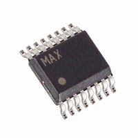
MAX8543EEE+ Maxim Integrated Products, MAX8543EEE+ Datasheet - Page 16

MAX8543EEE+
Manufacturer Part Number
MAX8543EEE+
Description
IC CNTRLR STEP DOWN 16-QSOP
Manufacturer
Maxim Integrated Products
Type
Step-Down (Buck)r
Datasheet
1.MAX8543EEE.pdf
(27 pages)
Specifications of MAX8543EEE+
Internal Switch(s)
No
Synchronous Rectifier
No
Number Of Outputs
1
Voltage - Output
0.8 ~ 11 V
Current - Output
25A
Frequency - Switching
200kHz ~ 1MHz
Voltage - Input
3 ~ 13.2 V
Operating Temperature
-40°C ~ 85°C
Mounting Type
Surface Mount
Package / Case
16-QSOP
Power - Output
667mW
Output Voltage
0.8 V to 11.88 V
Output Current
25000 mA
Mounting Style
SMD/SMT
Switching Frequency
200 KHz to 1000 KHz
Maximum Operating Temperature
+ 85 C
Minimum Operating Temperature
- 40 C
Synchronous Pin
Yes
Topology
Buck
Lead Free Status / RoHS Status
Lead free / RoHS Compliant
Step-Down Controllers with Prebias Startup,
Lossless Sensing, Synchronization, and OVP
The MAX8543/MAX8544 step-down controllers use a
PWM, current-mode control scheme. An internal
transconductance amplifier establishes an integrated
error voltage. The heart of the PWM controller is an
open-loop comparator that compares the integrated
voltage-feedback signal against the amplified current-
sense signal plus the slope-compensation ramp, which
are summed into the main PWM comparator to pre-
serve inner-loop stability and eliminate inductor stair-
casing. At each rising edge of the internal clock, the
high-side MOSFET turns on until the PWM comparator
trips or the maximum duty cycle is reached or the peak
current limit is reached. During this on-time, current
ramps up through the inductor, storing energy in a
magnetic field and sourcing current to the output. The
current-mode feedback system regulates the peak
inductor current as a function of the output-voltage-
error signal. The circuit acts as a switch-mode
transconductance amplifier and pushes the output LC
filter pole normally found in a voltage-mode PWM to a
higher frequency.
During the second half of the cycle, the high-side
MOSFET turns off and the low-side MOSFET turns on.
The inductor releases the stored energy as the current
ramps down, providing current to the output. The out-
put capacitor stores charge when the inductor current
exceeds the required load current and discharges
when the inductor current is lower, smoothing the volt-
age across the load. Under soft-overload conditions,
when the peak inductor current exceeds the selected
current limit (see the Current-Limit Circuit section), the
high-side MOSFET is turned off immediately and the
low-side MOSFET is turned on and remains on to let the
inductor current ramp down until the next clock cycle.
Under heavy-overload or short-circuit conditions, the
valley foldback current limit is enabled to reduce power
dissipation of external components.
The MAX8543/MAX8544 operate in a forced-PWM
mode. As a result, the controller maintains a constant
switching frequency, regardless of load, to allow for
easier filtering of the switching noise.
All MAX8543/MAX8544 functions are powered from the
on-chip, low-dropout, 5V linear regulator. Connect a
1µF to 10µF ceramic capacitor from VL to PGND. In
applications where the input voltage is less than 5.5V,
bypass the linear regulator by connecting VL to IN.
16
______________________________________________________________________________________
DC-DC Converter Control Architecture
Internal 5V Linear Regulator (VL)
Detailed Description
When VL drops below 2.62V, the MAX8543/MAX8544
assume that the supply voltage is too low for proper oper-
ation, so the undervoltage-lockout (UVLO) circuitry
inhibits switching and forces the DL and DH gate drivers
low. When VL rises above 2.7V, the controller enters the
startup sequence and then resumes normal operation.
The soft-start circuitry gradually ramps up the reference
voltage to control the rate of rise of the step-down con-
troller output and reduce input surge currents during
startup. The soft-start period is determined by the value
of the capacitor from SS to GND. The soft-start time is
approximately (33ms/µF) x C
also feature prebias startup; therefore, both external
power MOSFETs are kept off if the voltage at FB is higher
than that at SS. This allows the MAX8543/MAX8544 to
start up into a prebiased output without pulling the output
voltage down.
Before the MAX8543/MAX8544 can begin the soft-start
and power-up sequence, the following conditions must
be met:
1) V
2) EN is at logic high.
3) The thermal limit is not exceeded.
The MAX8543/MAX8544 feature a low-power shutdown
mode. A logic low at EN shuts down the controller.
During shutdown, the output is high impedance, and
both DH and DL are low. Shutdown reduces the quies-
cent current (I
enables the controller.
Synchronous rectification reduces conduction losses in
the rectifier by replacing the normal Schottky catch
diode with a low-resistance MOSFET switch. The
MAX8543/MAX8544 also use the synchronous rectifier
to ensure proper startup of the boost gate-driver circuit
and to provide the current-limit signal. The DL low-side
gate-drive waveform is always the complement of the
DH high-side gate-drive waveform (with controlled
dead time to prevent cross-conduction or shoot-
through). An adaptive dead-time circuit monitors the DL
voltage and prevents the high-side MOSFET from turn-
ing on until DL is fully off. For the dead-time circuit to
work properly, there must be a low-resistance, low-
inductance path from the DL driver to the MOSFET
gate. Otherwise, the sense circuitry in the MAX8543/
MAX8544 can interpret the MOSFET gate as off when
gate charge actually remains.
VL
exceeds the 2.7V undervoltage-lockout threshold.
Synchronous-Rectifier Driver (DL)
Q
) to less than 10µA. A logic high at EN
Undervoltage Lockout
Startup and Soft-Start
SS
. The MAX8543/MAX8544
Enable


