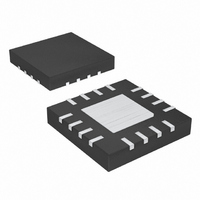
MAX5093AATE+ Maxim Integrated Products, MAX5093AATE+ Datasheet - Page 13

MAX5093AATE+
Manufacturer Part Number
MAX5093AATE+
Description
IC REG LDO W/BOOST 16TQFN
Manufacturer
Maxim Integrated Products
Type
Step-Up (Boost)r
Datasheet
1.MAX5092AATE.pdf
(24 pages)
Specifications of MAX5093AATE+
Internal Switch(s)
Yes
Synchronous Rectifier
No
Number Of Outputs
2
Voltage - Output
3.3V, 1.5 ~ 10 V
Current - Output
250mA
Voltage - Input
3.5 ~ 72 V
Operating Temperature
-40°C ~ 125°C
Mounting Type
Surface Mount
Package / Case
16-TQFN Exposed Pad
Power - Output
2.67W
Polarity
Positive
Input Voltage Max
72 V
Output Voltage
1.5 V to 10 V or 3.3 V
Output Type
Adjustable, Fixed
Dropout Voltage (max)
1.6 V @ 250 mA
Output Current
0.25 A (Min)
Line Regulation
1.6 mV/V (Typ)
Load Regulation
0.2 mV/mA (Typ)
Voltage Regulation Accuracy
1.5 %
Maximum Power Dissipation
2666 mW
Maximum Operating Temperature
+ 125 C
Mounting Style
SMD/SMT
Minimum Operating Temperature
- 40 C
Reference Voltage
1.235 V (Typ)
Lead Free Status / RoHS Status
Lead free / RoHS Compliant
Frequency - Switching
-
Lead Free Status / Rohs Status
Lead free / RoHS Compliant
An internal regulator (VL) is used to supply all internal
low-voltage blocks. Bypass VL to SGND with a 1µF
ceramic capacitor placed as close to the IC as possi-
ble. V
V
below 5.5V.
The MAX5092_/MAX5093_ contain an open-drain output
(RESET) that indicates when the LDO output (V
out of regulation. If the output of the LDO falls below 90%
of the nominal output voltage, RESET pulls low after a
short delay. Once the output rises above 92% of the
nominal output voltage, RESET goes high impedance
after the programmed reset timeout period. Connect a
100kΩ pullup resistor from OUT to RESET. See the CT
Capacitor Selection section for details on setting the
RESET timeout period.
Figure 3. Enable and Hold Timing Diagram
Table 1. Truth Table for Enable and Hold Timing Diagram
ORDER
VL
ORDER
1
2
3
4
5
5
4V to 72V Input LDOs with Boost Preregulator
tracks the voltage at BSOUT when V
HOLD
VL
OUT
EN
regulates to 5.5V when V
High
High
High
1
Low
Low
Low
EN
Power-On-Reset Output ( RESET )
Released
Released
Released
2
______________________________________________________________________________________
HOLD
Low
X
X
Internal Regulator (VL)
3
OUT
Off
On
Off
On
Off
On
BSOUT
Initial State. EN has a 500nA pulldown to GND. HOLD has an internal current source to OUT.
HOLD follows OUT.
Regulator output is active when EN is pulled high. HOLD is in release state, and it follows
OUT.
HOLD is in release state. OUT follows EN.
HOLD is pulled low externally after OUT turns on. The regulator output is forced on
regardless of the state of EN. A self-holding state.
HOLD is released after EN is pulled low. Output turns off.
Regulator enabled. Normal turn-on behavior. Regulator follows EN and HOLD follows OUT.
4
is above 5.5V.
BSOUT
OUT
) is
is
The MAX5092_/MAX5093_ utilize two logic inputs, EN
(active-high) and HOLD (active low), to implement a
self-holding circuit with no additional components. For
example, an automotive ignition switch drives EN high
and the regulator turns on. If HOLD is then driven low,
the regulator remains on even if EN goes low. As long
as HOLD is forced low and remains low after initial reg-
ulator power-up, the regulator remains on. From this
state, release HOLD (an internal current source con-
nects HOLD to OUT), or connect HOLD to OUT to turn
the regulator off. Drive EN low and HOLD high to place
the IC into shutdown mode. Shutdown mode reduces
supply current to 5µA. Figure 3 shows the timing dia-
gram for the enable and hold functions. Table 1 shows
the state of the regulator output with respect to the volt-
age level at EN and HOLD with reference to Figure 3.
Connect HOLD to OUT or leave unconnected to dis-
able the hold feature and use EN as a standard on/off
control input.
COMMENTS
Enable and Hold Inputs
5
6
13


