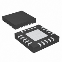
MAX8643AETG+ Maxim Integrated Products, MAX8643AETG+ Datasheet - Page 2

MAX8643AETG+
Manufacturer Part Number
MAX8643AETG+
Description
IC REG STP DWN 3A 24-TQFN
Manufacturer
Maxim Integrated Products
Type
Step-Down (Buck)r
Datasheet
1.MAX8643AETG.pdf
(16 pages)
Specifications of MAX8643AETG+
Internal Switch(s)
Yes
Synchronous Rectifier
Yes
Number Of Outputs
1
Voltage - Output
0.6 ~ 3.2 V
Current - Output
3A
Frequency - Switching
500kHz ~ 2MHz
Voltage - Input
2.35 ~ 3.6 V
Operating Temperature
-40°C ~ 85°C
Mounting Type
Surface Mount
Package / Case
24-TQFN Exposed Pad
Power - Output
2.22W
Lead Free Status / RoHS Status
Lead free / RoHS Compliant
ABSOLUTE MAXIMUM RATINGS
IN, V
COMP, FB, REFIN, OUT,
LX Current (Note 1) .....................................................-4A to +4A
BST to LX..................................................................-0.3V to +4V
PGND to GND .......................................................-0.3V to +0.3V
ELECTRICAL CHARACTERISTICS
(V
3A, 2MHz Step-Down Regulator
with Integrated Switches
Stresses beyond those listed under “Absolute Maximum Ratings” may cause permanent damage to the device. These are stress ratings only, and functional
operation of the device at these or any other conditions beyond those indicated in the operational sections of the specifications is not implied. Exposure to
absolute maximum rating conditions for extended periods may affect device reliability.
2
Note 1: LX has internal clamp diodes to GND and IN. Applications that forward bias these diodes should take care not to exceed
IN/V
IN and V
IN Supply Current
V
Total Shutdown Current from IN
and V
V
Threshold
BST
BST Supply Current
PWM COMPARATOR
PWM Comparator Propagation
Delay
COMP
COMP Clamp Voltage, High
COMP Slew Rate
PWM Ramp Amplitude
COMP Shutdown Resistance
ERROR AMPLIFIER
Preset Output-Voltage Accuracy
FB Regulation Accuracy Using
External Resistors
FB to OUT Resistor
CTL_, EN, SS, FREQ to GND...................-0.3V to (V
IN
DD
DD
_______________________________________________________________________________________
= V
DD
DD
Supply Current
Undervoltage Lockout
DD
, PWRGD to GND ......................................-0.3V to +4.5V
DD
the IC’s package power dissipation limits.
DD
= 3.3V, V
PARAMETER
Voltage Range
FB
= 0.5V, T
A
= -40°C to +85°C. Typical values are at T
f
(includes gate-drive current)
f
V
LX starts/stops switching
V
V
10mV overdrive
V
From COMP to GND, V
REFIN = SS
CTL1 = CTL2 = GND
All VID settings except CTL1 = CTL2 = GND
S
S
IN
BST
LX
IN
= 1MHz
= 1MHz, no load
= V
= 2.35V to 3.6V
= 3.6V or 0V, V
= V
DD
DD
= V
= V
BST
IN
DD
- V
= 3.6V,
+ 0.3V)
EN
LX
CONDITIONS
= 0V
EN
= 3.6V, V
= V
SS
= 0V
Continuous Power Dissipation (T
Operating Temperature Range ...........................-40°C to +85°C
Junction Temperature ......................................................+150°C
Storage Temperature Range .............................-65°C to +150°C
Lead Temperature (soldering, 10s) .................................+300°C
EN
V
V
V
V
V
V
Deglitching
T
T
A
A
IN
IN
IN
IN
DD
DD
24-Pin TQFN-EP
(derated 27.8mW/°C above +70°C)........................2222.2mW
= 0V
A
= +25°C
= +85°C
= 2.5V
= 3.3V
= 2.5V
= 3.3V
= +25°C, circuit of Figure 1, unless otherwise noted.) (Note 2)
rising
falling
0.594
MIN
2.35
1.8
-1
5
A
= +70°C)
Table 1
Select
0.600
TYP
from
5.5
1.4
1.9
1.4
10
20
4
2
2
2
2
1
8
8
0.606
MAX
3.60
4.6
2.3
2.1
13
+1
11
5
UNITS
V/µs
mA
mA
µA
kΩ
µA
µs
ns
%
Ω
V
V
V
V
V


