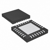
MAX15021ATI+ Maxim Integrated Products, MAX15021ATI+ Datasheet - Page 16

MAX15021ATI+
Manufacturer Part Number
MAX15021ATI+
Description
IC REG SYNC DUAL 28-TQFN-EP
Manufacturer
Maxim Integrated Products
Type
Step-Down (Buck)r
Datasheet
1.MAX15021ATI.pdf
(23 pages)
Specifications of MAX15021ATI+
Internal Switch(s)
Both
Synchronous Rectifier
Yes
Number Of Outputs
2
Voltage - Output
0.6 ~ 5.5 V
Current - Output
2A, 4A
Frequency - Switching
500kHz ~ 4MHz
Voltage - Input
2.5 ~ 5.5 V
Operating Temperature
-40°C ~ 125°C
Mounting Type
Surface Mount
Package / Case
28-TQFN Exposed Pad
Power - Output
2.76W
Topology
Buck
Output Voltage
0.6 V to 5.5 V
Output Current
2 A, 4 A
Input Voltage
2.5 V to 5.5 V
Duty Cycle (max)
100 %
Switching Frequency
500 KHz to 4 MHz
Maximum Operating Temperature
+ 125 C
Mounting Style
SMD/SMT
Minimum Operating Temperature
- 40 C
Operating Supply Voltage
2.5 V to 5.5 V
Lead Free Status / RoHS Status
Lead free / RoHS Compliant
As seen in Figure 4b, a Type II compensator provides for
stable closed-loop operation, leveraging the +20dB/
decade slope of the capacitor’s ESR zero, while extend-
ing the closed-loop gain-bandwidth of the regulator. The
zero crossover now occurs at approximately three times
the uncompensated crossover frequency, f
The Type II compensator’s midfrequency gain (approxi-
mately 12dB shown here) is designed to compensate
for the power modulator’s attenuation at the desired
crossover frequency, f
f
-20dB/decade rolloff above the ESR zero (f
leveraged to extend the active regulation gain-band-
width of the voltage regulator. As shown in Figure 4b,
the net result is a three times increase in the regulator’s
gain bandwidth while providing greater than 75° of
phase margin (the difference between Gain
Gain
Other filter schemes pose their own problems. For
instance, when choosing high-quality filter capacitor(s),
e.g. MLCCs, the inherent ESR zero may occur at a
much higher frequency, as shown in Figure 4c.
As with the previous example, the actual gain and
phase response is overlaid on the power modulator’s
asymptotic gain response. One readily observes the
more dramatic gain and phase transition at or near the
power modulator’s resonant frequency, f
Dual, 4A/2A, 4MHz, Step-Down DC-DC
Regulator with Tracking/Sequencing Capability
16
Figure 4c. Power Modulator Gain and Phase Response with
Low-Parasitic Capacitor(s) (MLCCs)
CO
). In this example, the power modulator’s inherent
MOD
______________________________________________________________________________________
-20
-40
-60
-80
respective phases at crossover, f
40
20
0
10
100
|G
< G
CO
1k
MOD
ASYMPTOTE
FREQUENCY (Hz)
MOD
|G
|
(Gain
MOD
10k
|
f
LC
E/A
100k
+ Gain
MAX15021 fig04c
1M
f
ESR
LC
CO
MOD
10M
CO
ZERO,ESR
, versus the
90
45
0
-45
-90
-135
-180
.
).
= 0dB at
E/A
and
) is
gentler response of the previous example. This is due
to the filter components’ lower parasitic (DCR and ESR)
and corresponding higher frequency of the inherent
ESR zero. In this example, the desired crossover fre-
quency occurs below the ESR zero frequency.
In this example, a compensator with an inherent midfre-
quency double-zero response is required to mitigate
the effects of the filter’s double-pole phase lag. This is
available with the Type III topology.
As demonstrated in Figure 4d, the Type III’s midfre-
quency double-zero gain (exhibiting a +20dB/dec
slope, noting the compensator’s pole at the origin) is
designed to compensate for the power modulator’s
double-pole -40dB/decade attenuation at the desired
crossover frequency, f
0dB at f
In the above example the power modulator’s inherent
(midfrequency) -40dB/decade rolloff is mitigated by the
midfrequency double zero’s +20dB/decade gain to
extend the active regulation gain-bandwidth of the volt-
age regulator. As shown in Figure 4d, the net result is
an approximate doubling in the controller’s gain band-
width while providing greater than 55 degrees of phase
margin (the difference between Gain
respective phases at crossover, f
Design procedures for both Type II and Type III com-
pensators are shown below.
Figure 4d. Power Modulator and Type III Compensator Gain
and Phase Response with Low Parasitic Capacitors (MLCCs)
CO
-20
-40
-60
-80
80
60
40
20
) (see Figure 4d).
0
10
|G
EA
|
100
CO
1k
< G
FREQUENCY (Hz)
< G
MOD
(again, Gain
EA
10k
f
LC
100k
CO
).
MAX15021 fig04d
E/A
1M
f
E/A
ESR
|G
f
CO
MOD
and Gain
+ Gain
10M
|
270
203
135
68
0
-68
-135
-203
-270
MOD
MOD
=


