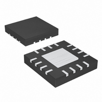
MAX5088ATE+ Maxim Integrated Products, MAX5088ATE+ Datasheet - Page 2

MAX5088ATE+
Manufacturer Part Number
MAX5088ATE+
Description
IC DC-DC CONV BUCK 16TQFN
Manufacturer
Maxim Integrated Products
Type
Step-Down (Buck)r
Datasheet
1.MAX5089ATE.pdf
(24 pages)
Specifications of MAX5088ATE+
Internal Switch(s)
Yes
Synchronous Rectifier
No
Number Of Outputs
1
Voltage - Output
0.6 ~ 20 V
Current - Output
2A
Frequency - Switching
200kHz ~ 2.2MHz
Voltage - Input
4.5 ~ 23 V
Operating Temperature
-40°C ~ 125°C
Mounting Type
Surface Mount
Package / Case
16-TQFN Exposed Pad
Power - Output
2.67W
Lead Free Status / RoHS Status
Lead free / RoHS Compliant
ABSOLUTE MAXIMUM RATINGS
V+ to PGND............................................................-0.3V to +25V
BST/VDD, DRAIN to SGND ....................................-0.3V to +30V
SGND to PGND .....................................................-0.3V to +0.3V
BST/VDD to SOURCE...............................................-0.3V to +6V
SOURCE to SGND..................................................-0.6V to +25V
SOURCE or DRAIN Maximum Peak Current...............5A for 1ms
V
SYNC, EN, DL, CKO, OSC, COMP,
BYPASS, CKO, OSC, COMP, FB, EN, SYNC, RESET,
ELECTRICAL CHARACTERISTICS
(V+ = V
values are at T
2.2MHz, 2A Buck Converters with an
Integrated High-Side Switch
*As per JEDEC51 Standard (multilayer board).
Stresses beyond those listed under “Absolute Maximum Ratings” may cause permanent damage to the device. These are stress ratings only, and functional
operation of the device at these or any other conditions beyond those indicated in the operational sections of the specifications is not implied. Exposure to
absolute maximum rating conditions for extended periods may affect device reliability.
2
SYSTEM SPECIFICATIONS
Input Voltage Range
V+ Operating Supply Current
V+ Standby Supply Current
Efficiency
V
V
V
Hysteresis
V
BYPASS Output Voltage
BYPASS Load Regulation
L
FB to SGND...............................................-0.3V to (V
PGOOD Maximum Input Current .................................±50mA
L
L
L
L
to SGND ................-0.3V to the lower of +6V and (V+ + 0.3V)
Undervoltage Lockout
Undervoltage Lockout
Output Voltage
_______________________________________________________________________________________
REGULATOR (V
L
= 5V or V+ = 5.5V to 23V, V
PARAMETER
A
= T
J
= +25°C.) (Note 1)
L
)/BYPASS OUTPUT (BYPASS)
EN
∆V
SYMBOL
V
= 5V, T
V
V
BYPASS
I
BYPASS
STBY
UVLO
HYST
V+
V
I
η
Q
L
A
= T
V+ = V
V+ = 12V, V
R
V+ = 12V, V
RESET, CKO unconnected (MAX5088),
R
Nonsynchronous (MAX5088),
f
V
Synchronous (MAX5089),
f
V
V
V+ = 5.5V to 23V, I
V+ = V
I
V+ = V
J
SW
SW
BYPASS
OUT
OUT
L
OSC
OSC
= -40°C to +125°C, unless otherwise noted. Circuits of Figures 5 and 6. Typical
L
falling
+ 0.3V)
= 1.25MHz, V+ = 12V, I
= 300kHz, V+ = 12V, I
= 3.3V
= 3.3V
= 10kΩ, no switching
= 10kΩ
L
L
L
= 5.2V
steps from 0 to 50µA,
= 5.2V
FB
EN
CONDITIONS
= 0.8V
= 0V, PGOOD (MAX5089),
RESET, PGOOD to SGND ........................................-0.3V to +6V
BYPASS to SGND..................................................-0.3V to +2.2V
V
Continuous Power Dissipation* (T
Package Thermal Resistance (junction to case) ............1.7°C/W
Operating Temperature Range .........................-40°C to +125°C
Junction Temperature Range ............................-65°C to +150°C
Storage Temperature Range .............................-65°C to +150°C
Lead Temperature (soldering, 10s) .................................+300°C
L
VL
16-Pin TQFN (derate 33mW/°C above +70°C) ..........2666mW
and BYPASS Short-Circuit Duration to SGND ......Continuous
= 0 to 40mA
OUT
OUT
= 1.5A,
= 1.5A,
1.98
MIN
5.5
4.5
5.0
0
A
= +70°C)
TYP
137
1.8
4.1
5.2
1.2
79
90
1
2
MAX
23.0
2.02
5.5
2.5
1.4
4.3
5.5
10
UNITS
mA
mA
mV
mV
%
V
V
V
V
V


