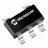
TC105303ECTTR Microchip Technology, TC105303ECTTR Datasheet - Page 5

TC105303ECTTR
Manufacturer Part Number
TC105303ECTTR
Description
IC PFM/PWM CONTRLLER 3V SOT23A-5
Manufacturer
Microchip Technology
Type
Step-Down (Buck)r
Datasheet
1.TC105333ECTTR.pdf
(14 pages)
Specifications of TC105303ECTTR
Internal Switch(s)
No
Synchronous Rectifier
No
Number Of Outputs
1
Voltage - Output
3V
Current - Output
1A
Frequency - Switching
300kHz
Voltage - Input
0.9 ~ 2.2 V
Operating Temperature
-40°C ~ 85°C
Mounting Type
Surface Mount
Package / Case
SOT-23-5, SC-74A, SOT-25
Power - Output
150mW
Output Current
1.0 A
Mounting Style
SMD/SMT
Lead Free Status / RoHS Status
Lead free / RoHS Compliant
Available stocks
Company
Part Number
Manufacturer
Quantity
Price
Company:
Part Number:
TC105303ECTTR
Manufacturer:
MICROCHIP
Quantity:
12 000
Part Number:
TC105303ECTTR
Manufacturer:
MICROCHIP/微芯
Quantity:
20 000
3.8
EXT is a complementary output with a maximum ON
resistance of 22Ω to V
when low. It is designed to directly drive a P-channel
MOSFET or a PNP bipolar transistor through a base
current limiting resistor (Figure 4-2). A PNP transistor is
recommended in applications where V
2.5V. Otherwise, a P-channel MOSFET is preferred as
it affords the highest efficiency because it does not
draw any gate drive current. However, P-channel
MOSFETs are typically more expensive than bipolar
transistors.
P-channel MOSFET selection is determined mainly by
the on-resistance, gate-source threshold, and gate
charge requirements. Also, the drain-to-source and
gate-to-source breakdown voltage ratings must be
greater than V
tion should be less than 100nC for best efficiency. The
MOSFET must be capable of handling the required
peak inductor current, and should have a very low
on-resistance at that current. For example, an Si9430
MOSFET has a drain-to-source rating of -20V, and a
typical on-resistance r
-4.5V. Table 4-1 lists suppliers of external components
recommended for use with the TC105.
©
2002 Microchip Technology Inc.
External Switching Transistor
Selection
DD
MAX
. The total gate charge specifica-
DD
DS
ON
when high and 19Ω to ground
of 0.07Ω at 2A, with V
IN
is less than
GS
=
3.8.1
As with all inductive switching regulators, the TC105
generates fast switching waveforms, which radiate
noise. Interconnecting lead lengths should be mini-
mized to keep stray capacitance, trace resistance and
radiated noise as low as possible. In addition, the GND
pin, input bypass capacitor and output filter capacitor
ground leads should be connected to a single point.
The input capacitor should be placed as close to power
and ground pins of the TC105 as possible. The length
of the EXT trace must also be kept as short as possible.
BOARD LAYOUT GUIDELINES
DS21349B-page 5
TC105


