LT1109CZ-12#PBF Linear Technology, LT1109CZ-12#PBF Datasheet - Page 4
LT1109CZ-12#PBF
Manufacturer Part Number
LT1109CZ-12#PBF
Description
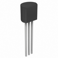
IC DC/DC CONV 12V TO-92-3
Manufacturer
Linear Technology
Type
Step-Up (Boost)r
Datasheet
1.LT1109CS8-12PBF.pdf
(8 pages)
Specifications of LT1109CZ-12#PBF
Internal Switch(s)
Yes
Synchronous Rectifier
No
Number Of Outputs
1
Voltage - Output
12V
Current - Output
100mA
Frequency - Switching
120kHz
Voltage - Input
3V, 5V
Operating Temperature
0°C ~ 70°C
Mounting Type
Through Hole
Package / Case
TO-92-3 (Standard Body), TO-226
Power - Output
300mW
Lead Free Status / RoHS Status
Lead free / RoHS Compliant


LT1109
4
The LT1109Z-5 and LT1109Z-12 are fixed output voltage
step-up DC/DC converters in a 3-pin TO-92 package.
Power for internal regulator circuitry is taken from the
V
operation can be best understood by referring to the block
diagram. V
negative input of comparator A1. When this voltage falls
below the 1.25V reference voltage, the oscillator is turned
on and the power switch Q1 cycles at the oscillator
BLOCK
TYPICAL PERFOR
LT1109Z
OUT
160
150
140
130
120
110
100
90
80
REFERENCE
2.0
1.25V
Minimum/Maximum
Oscillator Frequency vs t
V
GND
pin, a technique known as “bootstrapping.” Circuit
OUT
2.5
OUT
3.0
I D AGRA
, attenuated by R1 and R2, is applied to the
3.5
OPER
R1
R2
250k
T
LT1109-5, -12 Z Package
ON
4.0
T
+
–
( s)
A
= 25 C
LT1109-12: R1 = 29k
0 C T
A1
4.5
LT1109-5: R1 = 83k
COMPARATOR
ATIO
W
5.0
ON
A
LT1109 • TPC08
W
70 C
S
5.5
A
U
6.0
OSCILLATOR
U
120kHz
CE
C
450
400
350
300
250
200
HARA TERISTICS
DRIVER
Quiescent Current
0
T
LT1109 • TA03
A
2
= 25°C
4
C
SW
INPUT VOLTAGE (V)
6
Q1
8
10
frequency of 120kHz. Switch cycling alternately builds
current in the inductor, then dumps it into the output
capacitor, increasing the output voltage. When A1’s nega-
tive input rises above 1.25V, it turns off the oscillator. A
small amount of hysteresis in A1 obviates the need for
frequency compensation circuitry. When Q1 is off, current
into the V
from the battery will be higher because the device oper-
ates off the stepped-up voltage.
REFERENCE
12 14
1.25V
GND
ON FIXED VERSION PIN 8 IS SENSE
ON ADJUSTABLE VERSION PIN 8 IS FB AND R1 AND R2 ARE DISCONNECTED
V
IN
LT1109 • TPC09
16
FB
OUT
18
SENSE
20
pin drops to just 320 A. Quiescent current
LT1109-5, -12 N8, S8 Package
R1
R2
250k
+
–
A1
COMPARATOR
400
380
360
340
320
300
280
260
240
220
200
SHUTDOWN
–50
Quiescent Current
–25
TEMPERATURE (°C)
0
OSCILLATOR
120kHz
25
50
DRIVER
LT1109 • TPC10
75
LT1109 • TA04
100
SW
Q1
Related parts for LT1109CZ-12#PBF
Image
Part Number
Description
Manufacturer
Datasheet
Request
R

Part Number:
Description:
IC DC/DC CONV 12V TO-92-3
Manufacturer:
Linear Technology
Datasheet:
Part Number:
Description:
IC DC/DC CONV 5V TO-92-3
Manufacturer:
Linear Technology
Datasheet:
Part Number:
Description:
IC DC/DC CONV 5V TO-92-3
Manufacturer:
Linear Technology
Datasheet:

Part Number:
Description:
Micropower Low Cost DC/DC Converter Adjustable and Fixed 5V/ 12V
Manufacturer:
Linear Technology
Datasheet:
Part Number:
Description:
CD ROM LINEARVIEW DATASHEETS
Manufacturer:
Linear Technology

Part Number:
Description:
Standalone Linear Li-Ion Battery Charger with Thermal Regulation in ThinSOT
Manufacturer:
Linear Technology Corporation
Datasheet:
Part Number:
Description:
Low noise, high frequency, 8th order linear phase lowpass filter
Manufacturer:
Linear Technology Corporation
Datasheet:
Part Number:
Description:
Manufacturer:
Linear Technology Corporation
Datasheet:
Part Number:
Description:
Manufacturer:
Linear Technology Corporation
Datasheet:
Part Number:
Description:
Manufacturer:
Linear Technology Corporation
Datasheet:
Part Number:
Description:
Manufacturer:
Linear Technology Corporation
Datasheet:
Part Number:
Description:
Manufacturer:
Linear Technology Corporation
Datasheet:
Part Number:
Description:
Manufacturer:
Linear Technology Corporation
Datasheet:
Part Number:
Description:
Manufacturer:
Linear Technology Corporation
Datasheet:
Part Number:
Description:
Dual and Quad, JFET Input Precision High Speed Op Amps
Manufacturer:
Linear Technology Corporation
Datasheet: