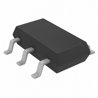
LTC1772BES6#TRPBF Linear Technology, LTC1772BES6#TRPBF Datasheet - Page 6

LTC1772BES6#TRPBF
Manufacturer Part Number
LTC1772BES6#TRPBF
Description
IC CTRLR DC/DC S-DWN SOT23-6
Manufacturer
Linear Technology
Type
Step-Down (Buck)r
Datasheet
1.LTC1772BES6TRMPBF.pdf
(16 pages)
Specifications of LTC1772BES6#TRPBF
Internal Switch(s)
No
Synchronous Rectifier
No
Number Of Outputs
1
Voltage - Output
0.8 ~ 9.8 V
Current - Output
1A
Frequency - Switching
550kHz
Voltage - Input
2.5 ~ 9.8 V
Operating Temperature
-40°C ~ 85°C
Mounting Type
Surface Mount
Package / Case
TSOT-23-6, TSOT-6
Lead Free Status / RoHS Status
Lead free / RoHS Compliant
Power - Output
-
Available stocks
Company
Part Number
Manufacturer
Quantity
Price
LTC1772B
OPERATION
Main Control Loop
The LTC1772B is a constant frequency current mode
switching regulator. During normal operation, the external
P-channel power MOSFET is turned on each cycle when
the oscillator sets the RS latch (RS1) and turned off when
the current comparator (ICMP) resets the latch. The peak
inductor current at which ICMP resets the RS latch is
controlled by the voltage on the I
output of the error amplifi er EAMP . An external resistive
divider connected between V
EAMP to receive an output feedback voltage V
the load current increases, it causes a slight decrease in
V
I
current matches the new load current.
The main control loop is shut down by pulling the I
pin low. Releasing I
source to charge up the external compensation network.
When the I
loop is enabled with the I
to its zero current level of approximately 0.85V. As the
external compensation network continues to charge up,
the corresponding output current trip level follows, allow-
ing normal operation.
Comparator OVP guards against transient overshoots
> 7.5% by turning off the external P-channel power
MOSFET and keeping it off until the fault is removed.
6
TH
FB
/RUN voltage to increase until the average inductor
relative to the 0.8V reference, which in turn causes the
20mV
AC
/DIV
TH
V
LTC1772 Burst Mode Operation.
V
V
I
/RUN pin reaches 0.35V, the main control
OUT
IN
OUT
OUT
= 3.6V
= 100mA
= 2.5V
Ripple for Figure 1 Circuit Using
TH
/RUN allows an internal 0.5μA current
(Refer to Functional Diagram)
TH
/RUN voltage then pulled up
5μs/DIV
OUT
Figure 2. Output Ripple Waveforms for the Circuit of Figure 1.
TH
and ground allows the
/RUN pin, which is the
1772 F02a
FB
TH
. When
/RUN
Low Load Current Operation
Under very light load current conditions, the I
voltage will be very close to the zero current level of 0.85V.
As the load current decreases further, an internal offset at
the current comparator input will assure that the current
comparator remains tripped (even at zero load current) and
the regulator will start to skip cycles, as it must, in order
to maintain regulation. This behavior allows the regulator
to maintain constant frequency down to very light loads,
resulting in less low frequency noise generation over a
wide load current range.
Figure 2 illustrates this result for the circuit of Figure 1
using both an LTC1772 in Burst Mode operation and an
LTC1772B (non-Burst Mode operation). At an output cur-
rent of 100mA, the Burst Mode operation part exhibits
an output ripple of approximately 60mV
non-Burst Mode operation part has an output ripple of only
20mV
is even greater. This comes at a tradeoff of lower effi ciency
for the non-Burst Mode operation part (see Figure 1). Also
notice the constant frequency operation of the LTC1772B,
even at 5% of maximum output current.
Dropout Operation
When the input supply voltage decreases towards the
output voltage, the rate of change of inductor current
during the ON cycle decreases. This reduction means
20mV
P-P
AC
. At lower output current levels, the improvement
/DIV
V
LTC1772B Non-Burst Mode Operation.
V
V
I
OUT
OUT
IN
OUT
= 3.6V
= 100mA
= 2.5V
Ripple for Figure 1 Circuit Using
5μs/DIV
P-P
, whereas the
1772 F02b
TH
/RUN pin
1772bfa


