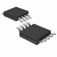
LTC1503CMS8-1.8 Linear Technology, LTC1503CMS8-1.8 Datasheet - Page 9

LTC1503CMS8-1.8
Manufacturer Part Number
LTC1503CMS8-1.8
Description
IC BUCK/SW CAP 1.8V .1A 8MSOP
Manufacturer
Linear Technology
Type
Step-Down (Buck), Switched Capacitor (Charge Pump)r
Datasheet
1.LTC1503CS8-1.8PBF.pdf
(12 pages)
Specifications of LTC1503CMS8-1.8
Internal Switch(s)
Yes
Synchronous Rectifier
No
Number Of Outputs
1
Voltage - Output
1.8V
Current - Output
100mA
Frequency - Switching
600kHz
Voltage - Input
2.4 ~ 6 V
Operating Temperature
-40°C ~ 85°C
Mounting Type
Surface Mount
Package / Case
8-MSOP, Micro8™, 8-uMAX, 8-uSOP,
Lead Free Status / RoHS Status
Contains lead / RoHS non-compliant
Power - Output
-
Available stocks
Company
Part Number
Manufacturer
Quantity
Price
Company:
Part Number:
LTC1503CMS8-1.8
Manufacturer:
LT
Quantity:
5 321
Company:
Part Number:
LTC1503CMS8-1.8
Manufacturer:
LT
Quantity:
10 000
Part Number:
LTC1503CMS8-1.8
Manufacturer:
LINEAR/凌特
Quantity:
20 000
Part Number:
LTC1503CMS8-1.8#PBF
Manufacturer:
LINEAR/凌特
Quantity:
20 000
Company:
Part Number:
LTC1503CMS8-1.8#TRPBF
Manufacturer:
LINEAR
Quantity:
9 817
Part Number:
LTC1503CMS8-1.8#TRPBF
Manufacturer:
LINEAR/凌特
Quantity:
20 000
APPLICATIO S I FOR ATIO
capacitor on V
quency ripple. An RC filter may also be used to reduce high
frequency voltage spikes.
Protection Features
The LTC1503-X contains both thermal shutdown and
short-circuit protection features. The charge pump will
shut down when the junction temperature reaches ap-
proximately 150 C and will resume operation once the
junction temperature has dropped back to 125 C. The part
will limit output current to 20mA (typ) when a short-circuit
condition (V
internal switches. During start-up, the 20mA current limit
Figure 3. Output Ripple Reduction Techniques
LTC1503-X
LTC1503-X
OUT
V
V
OUT
OUT
OUT
< 150mV) exists to prevent damage to the
to reduce both the low and high fre-
U
+
+
10 F
TANTALUM
10 F
TANTALUM
U
0.5
+
W
10 F
TANTALUM
1 F
CERAMIC
1503-1.8/2 F03
V
V
OUT
OUT
U
is disabled once V
survive an indefinite short from V
Layout Considerations
For best regulation and noise performance, careful board
layout is required. Improper bypassing and grounding
may lead to poor load regulation and output ripple perfor-
mance. All capacitors, especially C
close as possible to the V
GND pin and all bypass capacitors to an uninterrupted
ground plane is also advised. See Figure 4 for recom-
mended component placement and grounding.
Figure 4. Recommended Component Placement and Grounding
LTC1503-1.8/LTC1503-2
V
C1
OUT
V
IN
OUT
C
C
OUT
reaches 0.7V (typ). The part can
IN
IN
LTC1503-X
GND
and V
OUT
OUT
IN
and C
pins. Connecting the
to GND.
SHDN/SS
1503-1.8/2 F04
C2
OUT
, must be as
9


