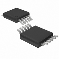
LT1945EMS Linear Technology, LT1945EMS Datasheet - Page 4

LT1945EMS
Manufacturer Part Number
LT1945EMS
Description
IC DC/DC CONV MICRPWR DUAL10MSOP
Manufacturer
Linear Technology
Type
Step-Up (Boost), Inverting, Flyback, Sepicr
Datasheet
1.LT1945EMS.pdf
(8 pages)
Specifications of LT1945EMS
Internal Switch(s)
Yes
Synchronous Rectifier
No
Number Of Outputs
2
Voltage - Output
1.23 ~ 36 V
Current - Output
350mA
Voltage - Input
1.2 ~ 15 V
Operating Temperature
-40°C ~ 85°C
Mounting Type
Surface Mount
Package / Case
10-MSOP, Micro10™, 10-uMAX, 10-uSOP
Lead Free Status / RoHS Status
Contains lead / RoHS non-compliant
Power - Output
-
Frequency - Switching
-
Available stocks
Company
Part Number
Manufacturer
Quantity
Price
Company:
Part Number:
LT1945EMS
Manufacturer:
LT
Quantity:
10 000
Part Number:
LT1945EMS
Manufacturer:
LINEAR/凌特
Quantity:
20 000
Part Number:
LT1945EMS#PBF
Manufacturer:
LT/凌特
Quantity:
20 000
Company:
Part Number:
LT1945EMS#TR
Manufacturer:
LT
Quantity:
596
Part Number:
LT1945EMS#TRPBF
Manufacturer:
LTNEAR
Quantity:
20 000
Company:
Part Number:
LT1945EMS#TRPRF
Manufacturer:
LINEAR
Quantity:
500
PIN FUNCTIONS
LT1945
NFB1 (Pin 1): Feedback Pin for Switcher 1. Set the output
voltage by selecting values for R1 and R2.
SHDN1 (Pin 2): Shutdown Pin for Switcher 1. Tie this
pin to 0.9V or higher to enable device. Tie below 0.25V
to turn it off.
GND (Pin 3): Ground. Tie this pin directly to the local
ground plane.
SHDN2 (Pin 4): Shutdown Pin for Switcher 2. Tie this
pin to 0.9V or higher to enable device. Tie below 0.25V
to turn it off.
FB2 (Pin 5): Feedback Pin for Switcher 2. Set the output
voltage by selecting values for R1B and R2B.
BLOCK DIAGRAM
OPERATION
The LT1945 uses a constant off-time control scheme
to provide high effi ciencies over a wide range of output
current. Operation can be best understood by referring
to the block diagram in Figure 1. Q1 and Q2 along with
R3 and R4 form a bandgap reference used to regulate
the output voltage. When the voltage at the NFB1 pin is
4
(EXTERNAL)
(EXTERNAL)
R1
R2
V
V
IN
OUT1
NFB1
C1
1
8
Q1
R5
80k
V
IN
Q2
X10
R6
80k
R3
60k
R4
280k
+
–
2
SHDN1
A1
ONE-SHOT
SWITCHER 1
3
ENABLE
400ns
GND
L1
RESET
A2
+
–
10
DRIVER
Figure 1. LT1945 Block Diagram
C3
SW1
42mV
D1
Q3
0.12Ω
L2
9
PGND
C2
V
PGND
OUT1
SW2 (Pin 6): Switch Pin for Switcher 2. This is the
collector of the internal NPN power switch. Minimize the
metal trace area connected to the pin to minimize EMI.
PGND (Pins 7, 9): Power Ground. Tie these pins directly
to the local ground plane. Both pins must be tied.
V
capacitor as close to the device as possible.
SW1 (Pin 10): Switch Pin for Switcher 1. This is the
collector of the internal NPN power switch. Minimize the
metal trace area connected to the pin to minimize EMI.
slightly below –1.23V, comparator A1 disables most of
the internal circuitry. Output current is then provided by
capacitor C2, which slowly discharges until the voltage
at the NFB1 pin goes above the hysteresis point of A1
(typical hysteresis at the NFB1 pin is 8mV). A1 then enables
the internal circuitry, turns on power switch Q3, and the
IN
0.12Ω
7
Q3B
(Pin 8): Input Supply Pin. Bypass this pin with a
V
OUT2
42mV
C4
DRIVER
SW2
D2
+
–
6
A2B
SWITCHER 2
ONE-SHOT
ENABLE
400ns
L3
RESET
SHDN2
A1B
V
4
+
–
IN
140k
R6B
R3B
R4B
40k
Q2B
30k
X10
R5B
40k
Q1B
1945 BD
5
FB2
V
OUT2
V
IN
R1B
(EXTERNAL)
R2B
(EXTERNAL)
1945fa


