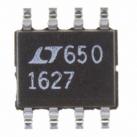
LTC1627CS8 Linear Technology, LTC1627CS8 Datasheet - Page 11

LTC1627CS8
Manufacturer Part Number
LTC1627CS8
Description
IC SW REG STEP-DOWN SYNC 8-SOIC
Manufacturer
Linear Technology
Type
Step-Down (Buck)r
Datasheet
1.LTC1627CS8PBF.pdf
(16 pages)
Specifications of LTC1627CS8
Internal Switch(s)
Yes
Synchronous Rectifier
Yes
Number Of Outputs
1
Voltage - Output
0.8 ~ 8.5 V
Current - Output
500mA
Frequency - Switching
35kHz ~ 350kHz
Voltage - Input
2.65 ~ 8.5 V
Operating Temperature
0°C ~ 70°C
Mounting Type
Surface Mount
Package / Case
8-SOIC (3.9mm Width)
Lead Free Status / RoHS Status
Contains lead / RoHS non-compliant
Power - Output
-
Available stocks
Company
Part Number
Manufacturer
Quantity
Price
Part Number:
LTC1627CS8
Manufacturer:
LT/凌特
Quantity:
20 000
Part Number:
LTC1627CS8#TR
Manufacturer:
LT/凌特
Quantity:
20 000
Part Number:
LTC1627CS8#TRPBF
Manufacturer:
LINEAR/凌特
Quantity:
20 000
APPLICATIO S I FOR ATIO
Checking Transient Response
The regulator loop response can be checked by looking at
the load transient response. Switching regulators take
several cycles to respond to a step in load current. When
a load step occurs, V
equal to ( I
resistance of C
charge C
regulator loop then acts to return V
value. During this recovery time V
overshoot or ringing that would indicate a stability prob-
lem. The internal compensation provides adequate com-
pensation for most applications. But if additional compen-
sation is required, the I
compensation as shown in Figure 7.
A second, more severe transient is caused by switching in
loads with large (>1 F) supply bypass capacitors. The
discharged bypass capacitors are effectively put in parallel
with C
deliver enough current to prevent this problem if the load
switch resistance is low and it is driven quickly. The only
solution is to limit the rise time of the switch drive so that
OUT
OUT
, causing a rapid drop in V
LOAD
, which generates a feedback error signal. The
OPTIONAL
OUT
• ESR), where ESR is the effective series
. I
U
OUT
LOAD
TH
immediately shifts by an amount
U
R
C
also begins to charge or dis-
pin can be used for external
C
C2
C
BOLD LINES INDICATE
HIGH CURRENT PATHS
SS
C
OUT
C1
W
OUT
OUT
can be monitored for
1
2
3
4
to its steady-state
. No regulator can
I
RUN/SS
V
GND
TH
FB
Figure 7. LTC1627 Layout Diagram
LTC1627
U
SYNC/FCB
V
SW
V
DR
IN
8
7
6
5
R2
R1
the load rise time is limited to approximately (25 • C
Thus, a 10 F capacitor would require a 250 s rise time,
limiting the charging current to about 130mA.
PC Board Layout Checklist
When laying out the printed circuit board, the following
checklist should be used to ensure proper operation of the
LTC1627. These items are also illustrated graphically in
the layout diagram of Figure 7. Check the following in your
layout:
1. Are the signal and power grounds segregated? The
2. Does the V
L1
LTC1627 signal ground consists of the resistive
divider, the optional compensation network (R
C
(–) plate of C
LTC1627. The power ground traces should be kept
short, direct and wide. The signal ground and power
ground should converge to a common node in a star-
ground configuration.
resistors? The resistive divider R1/R2 must be con-
nected between the (+) plate of C
C1
+
), C
C
OUT
SS
V
OUT
+
–
and C
FB
IN
, the (–) plate of C
pin connect directly to the feedback
C2
. The power ground consists of the
OPTIONAL
C
V
D1
D2
C
B
C
OUT
IN
1627 F07
OUT
+
and signal ground.
LTC1627
and Pin 4 of the
V
+
–
IN
11
LOAD
C
and
).


