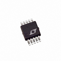
LTC3251EMSE Linear Technology, LTC3251EMSE Datasheet - Page 8

LTC3251EMSE
Manufacturer Part Number
LTC3251EMSE
Description
IC CONV DC/DC SDOWN HIEFF 10MSOP
Manufacturer
Linear Technology
Type
Step-Down (Buck), Switched Capacitor (Charge Pump)r
Datasheet
1.LTC3251EMSEPBF.pdf
(16 pages)
Specifications of LTC3251EMSE
Internal Switch(s)
Yes
Synchronous Rectifier
No
Number Of Outputs
1
Voltage - Output
0.9 ~ 1.6 V
Current - Output
500mA
Frequency - Switching
1MHz ~ 1.6MHz
Voltage - Input
2.7 ~ 5.5 V
Operating Temperature
-40°C ~ 85°C
Mounting Type
Surface Mount
Package / Case
10-MSOP Exposed Pad, 10-HMSOP, 10-eMSOP
Lead Free Status / RoHS Status
Contains lead / RoHS non-compliant
Power - Output
-
Other names
LTC3251EMS
LTC3251EMS
LTC3251EMS
Available stocks
Company
Part Number
Manufacturer
Quantity
Price
Company:
Part Number:
LTC3251EMSE
Manufacturer:
LT
Quantity:
10 000
Part Number:
LTC3251EMSE
Manufacturer:
LINEAR/凌特
Quantity:
20 000
Company:
Part Number:
LTC3251EMSE#PBF
Manufacturer:
LINEAR
Quantity:
429
Part Number:
LTC3251EMSE#TRPBF
Manufacturer:
LT/凌特
Quantity:
20 000
Part Number:
LTC3251EMSE-1.2
Manufacturer:
LINEAR/凌特
Quantity:
20 000
Company:
Part Number:
LTC3251EMSE-1.5
Manufacturer:
LT
Quantity:
10 000
Part Number:
LTC3251EMSE-1.5
Manufacturer:
LINEAR/凌特
Quantity:
20 000
OPERATIO
LTC3251/
LTC3251-1.2/LTC3251-1.5
The LTC3251 family of parts use a dual phase switched
capacitor charge pump to step down V
output voltage. Regulation is achieved by sensing the
output voltage through an external resistor divider and
modulating the charge pump output current based on the
error signal. A 2-phase nonoverlapping clock activates the
two charge pumps. The two charge pumps work in paral-
lel, but out of phase from each other. On the first phase of
the clock, current is transferred from V
external flying capacitor 1, to V
Charge Pump 1. Not only is current being delivered to V
on the first phase, but the flying capacitor is also being
charged. On the second phase of the clock, flying capaci-
tor 1 is connected from V
charge stored during the first phase of the clock to V
the switches of Charge Pump 1. Charge Pump 2 operates
in the same manner, but with the phases of the clock
reversed. This dual phase architecture achieves extremely
low output and input noise by providing constant charge
transfer from V
Using this method of switching, only half of the output
current is delivered from V
efficiency over a conventional LDO. A spread spectrum
oscillator, which utilizes random switching frequencies
between 1MHz and 1.6MHz, sets the rate of charging and
discharging of the flying capacitors. The LTC3251-1.2/
LTC3251-1.5 MODE pin can be used to disable spread
spectrum operation which causes switching to occur at
1.6MHz. The part also has two types of low current Burst
Mode operation to improve efficiency even at light loads.
In shutdown mode, all circuitry is turned off and the
LTC3251 family draws only leakage current from the V
supply. Furthermore, V
MD0 and MD1 pins are CMOS inputs with threshold
voltages of approximately 0.8V to allow regulator control
with low voltage logic levels. The MODE pin is also CMOS,
but has a threshold of about 1/2 • V
is in shutdown when a logic low is applied to both mode
pins. Since MD0, MD1 and MODE pins are high impedance
CMOS inputs, they should never be allowed to float.
Always drive MD0, MD1 and Mode with valid logic levels.
8
IN
U
to V
(Refer to Block Diagram)
OUT
OUT
.
OUT
is disconnected from V
IN
to ground, transferring the
, thus achieving twice the
OUT
IN
. The LTC3251 family
via the switches of
IN
IN
to a regulated
, through the
OUT
IN
. The
OUT
via
IN
Short-Circuit/Thermal Protection
The LTC3251 family has built-in short-circuit current
limiting as well as overtemperature protection. During
short-circuit conditions, internal circuitry automatically
limits the output current to approximately 800mA. At
higher temperatures, or in cases where internal power
dissipation causes excessive self heating on chip (i.e.,
output short circuit), the thermal shutdown circuitry will
shut down the charge pumps when the junction tempera-
ture exceeds approximately 160°C. It will re-enable the
charge pumps once the junction temperature drops back
to approximately 150°C. The LTC3251 will cycle in and out
of thermal shutdown without latch-up or damage until the
overstress condition is removed. Long term overstress
(I
can degrade the performance or shorten the life of the part.
Soft-Start
To prevent excessive current flow at V
the LTC3251 family has built-in soft-start circuitry. Soft-
start is achieved by increasing the amount of current
available to the output charge storage capacitor linearly
over a period of approximately 500µs. Soft-start is en-
abled whenever the device is brought out of shutdown,
and is disabled shortly after regulation is achieved.
Spread Spectrum Operation
Switching regulators can be particularly troublesome where
electromagnetic interference (EMI) is concerned. Switch-
ing regulators operate on a cycle-by-cycle basis to transfer
power to an output. In most cases the frequency of
operation is either fixed or is a constant based on the
output load. This method of conversion creates large
components of noise at the frequency of operation (funda-
mental) and multiples of the operating frequency (har-
monics). Figure 1a shows a conventional buck switching
converter. Figures 1b and 1c are the input and output noise
spectrums for the buck converter of Figure 1 with V
3.6V, V
OUT
> 650mA and/or T
OUT
= 1.5V and I
J
OUT
> 125°C) should be avoided as it
= 500mA.
IN
during start-up,
32511215fb
IN
=


