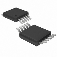
LTC3704IMS#PBF Linear Technology, LTC3704IMS#PBF Datasheet - Page 23

LTC3704IMS#PBF
Manufacturer Part Number
LTC3704IMS#PBF
Description
IC INV SYNC 5.2V 50MA 10MSOP
Manufacturer
Linear Technology
Type
Invertingr
Datasheet
1.LTC3704EMSPBF.pdf
(28 pages)
Specifications of LTC3704IMS#PBF
Internal Switch(s)
No
Synchronous Rectifier
No
Number Of Outputs
1
Voltage - Output
-5.2V
Current - Output
50mA
Frequency - Switching
50kHz ~ 1MHz
Voltage - Input
2.5 ~ 36 V
Operating Temperature
-40°C ~ 125°C
Mounting Type
Surface Mount
Package / Case
10-MSOP, Micro10™, 10-uMAX, 10-uSOP
Lead Free Status / RoHS Status
Lead free / RoHS Compliant
Power - Output
-
Available stocks
Company
Part Number
Manufacturer
Quantity
Price
APPLICATIO S I FOR ATIO
PC Board Layout Checklist
1. In order to minimize switching noise and improve
output load regulation, the GND pin of the LTC3704
should be connected directly to 1) the negative termi-
nal of the INTV
terminal of the output decoupling capacitors, 3) the
R2
OUTPUT SENSING
C
C
SIGNAL GROUND
PSEUDO-KELVIN
C2
C1
VIAS TO GROUND
PLANE
R
TRUE REMOTE
CONNECTION
T
R1
R
C
CC
C3
R3
U
decoupling capacitor, 2) the negative
BOLD LINES INDICATE HIGH CURRENT PATHS
PIN 1
LTC3704
R4
U
C
C
R2
C1
C2
Figure 22. LTC3704 Positive-to-Negative Converter Suggested Layout
C3
Figure 23. LTC3704 Positive-to-Negative Converter Layout Diagram
R1
R
GROUND CONNECTION
T
C
OUT
R
C
C
PSEUDO-KELVIN
VCC
W
R3
1
2
3
4
5
RUN
I
NFB
FREQ
MODE/
SYNC
TH
LTC3704
R4
C
C
OUT
IN
U
INTV
SENSE
GATE
GND
V
CC
IN
10
9
8
7
6
D1
M1
C
VCC
source of the power MOSFET or the bottom terminal of
the sense resistor, 4) the negative terminal of the input
capacitor and 5) at least one via to the ground plane
immediately adjacent to Pin 6. The ground trace on the
top layer of the PC board should be as wide and short
as possible to minimize series resistance and induc-
tance.
C
V
IN
OUT
L1
C
DC
V
IN
M1
C
DC
D1
L2
1
2
3
4
5
6
3704 F23
L1
L2
+
C
OUT
V
GND
V
IN
OUT
LTC3704
11
10
12
9
8
7
3704 F??
23
3704fb


