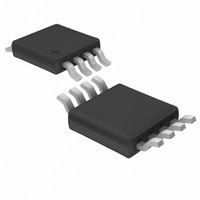
LT1612EMS8#TR Linear Technology, LT1612EMS8#TR Datasheet - Page 5

LT1612EMS8#TR
Manufacturer Part Number
LT1612EMS8#TR
Description
IC CONV DC/DC PWM STEPDOWN 8MSOP
Manufacturer
Linear Technology
Type
Step-Down (Buck)r
Datasheet
1.LT1612ES8.pdf
(12 pages)
Specifications of LT1612EMS8#TR
Internal Switch(s)
Yes
Synchronous Rectifier
Yes
Number Of Outputs
1
Voltage - Output
Adj to 0.6V
Current - Output
500mA
Frequency - Switching
800kHz
Voltage - Input
2 ~ 5.5 V
Operating Temperature
-40°C ~ 85°C
Mounting Type
Surface Mount
Package / Case
8-MSOP, Micro8™, 8-uMAX, 8-uSOP,
Lead Free Status / RoHS Status
Contains lead / RoHS non-compliant
Power - Output
-
Available stocks
Company
Part Number
Manufacturer
Quantity
Price
PIN
V
source output of the error amplifier. By connecting an RC
network from this pin to ground, frequency response can
be tuned for a wide range of circuit configurations. The
voltage at this pin also sets the current limit, and if
grounded, the switch will remain in the OFF state.
FB (Pin 2): Feedback Pin. This pin is the negative input to
the error amplifier. Connect the resistor divider tap to this
point which sets V
V
next to this pin.
GND (Pin 4): Ground Pin. Connect directly to local ground
plane.
BLOCK DIAGRA
MODE
SHDN
C
IN
V
U
V
(Pin 1): Compensation Pin. This is the current sink/
(Pin 3): Supply Pin. Bypass capacitor C1 must be right
V
FB
IN
OUT
C
7
FUNCTIONS
3
1
2
8
= 0.62V (1 + R1/R2)
U
0.62V
SHUTDOWN
OUT
–
+
U
A1
according to:
0.7V
W
OSCILLATOR
–
A3
ENABLE
+
V/I
+
R
0.08
SENSE
A2
–
SW (Pin 5): Switch Pin. Connect inductor and boost
capacitor here. Minimize trace area at this pin to keep EMI
down.
BOOST (Pin 6): This is the supply pin for the switch driver
and must be above V
tion. Connect the boost capacitor to this pin.
MODE (Pin 7): Burst Mode Operation Disable Pin. For
continuous switching operation (low noise), pull this pin
above 2V. For Burst Mode operation which gives better
light load efficiency, tie to ground. Output ripple voltage in
Burst Mode operation is typically 30mV
tions section for more information about this function.
SHDN (Pin 8): Shutdown Pin. Pull this pin low for shut-
down mode. Tie to a voltage between 2V and 5.5V for
normal operation.
R
FLIP-FLOP
S
Q
SLOPE
COMPENSATION
RECTIFIER
DRIVE
SWITCH
DRIVER
IN
by 1.5V for proper switch opera-
BOOST DIODE
SWITCH
RECTIFIER
P-P
. See applica-
LT1612
sn1612 1612fs
6
5
4
1612 BD
BOOST
SW
GND
5


