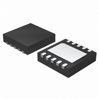
LTC3447EDD#TRPBF Linear Technology, LTC3447EDD#TRPBF Datasheet - Page 14

LTC3447EDD#TRPBF
Manufacturer Part Number
LTC3447EDD#TRPBF
Description
IC CONV DC/DC SYNC BUCK 10DFN
Manufacturer
Linear Technology
Type
Step-Down (Buck)r
Datasheet
1.LTC3447EDDPBF.pdf
(16 pages)
Specifications of LTC3447EDD#TRPBF
Internal Switch(s)
Yes
Synchronous Rectifier
Yes
Number Of Outputs
1
Voltage - Output
0.69 ~ 2.05 V
Current - Output
600mA
Frequency - Switching
1MHz
Voltage - Input
2.5 ~ 5.5 V
Operating Temperature
-40°C ~ 85°C
Mounting Type
Surface Mount
Package / Case
10-DFN
Lead Free Status / RoHS Status
Lead free / RoHS Compliant
Power - Output
-
Available stocks
Company
Part Number
Manufacturer
Quantity
Price
LTC3447
APPLICATIO S I FOR ATIO
junction temperature of the part. The temperature rise
is given by:
where P
θ
to the temperature.
The junction temperature, T
where T
As an example, consider the LTC3447 when using an input
voltage of 3.6V, an ambient temperature of 70°C, and a
buck load current of 500mA. From the typical performance
graph of switch resistance, the R
switch at 70°C is approximately 0.45Ω. Therefore, power
dissipated by the part is:
For the DFN-10 package, the θ
junction temperature of the regulator is:
which is well below the maximum junction temperature of
150°C. Note that at higher supply voltages, the junction
temperature is lower due to reduced switch resistance
(R
PC Board Layout Checklist
When laying out the printed circuit board, the following
checklist should be used to ensure proper operation of
the LTC3447. These items are also illustrated graphically
in Figures 9 and 10. Check the following in your layout:
1. The power traces, consisting of the GND trace, the
SW trace, and the V
and wide.
2. Does the V
reference? Ensure that there is no load current running
from the output voltage and the V
3. Does the FB pin connect directly to the feedback voltage
reference? Ensure that there is no load current running
from the feedback reference voltage and the FB pin.
4. Does the (+) plate of C
14
JA
DS(ON)
T
T
P
T
is the thermal resistance from the junction of the die
R
J
J
D
= T
= 70°C + (0.1125)(43) = 74.8°C
= θ
= I
A
D
).
A
LOAD
JA
is the ambient temperature.
is the power dissipated by the regulator and
+ T
• P
OUT
2
R
D
• R
pin connect directly to the output voltage
DS(ON)
U
IN
trace should be kept short, direct
= 112.5mW
IN
U
J
connect to V
, is given by:
JA
DS(ON)
OUT
is 43°C/W. Thus, the
W
sense pin.
of the P-channel
IN
as closely as
U
possible? This capacitor provides the AC current to the
internal power MOSFETs.
5. Keep the switching node, SW, away from the sensitive
V
6. Keep the (–) plates of C
sible.
OUT
V
IN
and FB nodes.
R1
R2
V
IN
Figure 10. LTC3447 Layout Diagram
Figure 9. LTC3447 Suggested Layout
C
R1
IN
GND PLANE
GND
FB
PGOOD
V
V
OUT
IN
R2
C
IN
GND
PGOOD
V
V
FB
OUT
IN
IN
and C
C
OUT
V
RUN
SDA
SCL
GND PLANE
CCD
SW
OUT
V
RUN
SDA
SCL
CCD
SW
as close as pos-
C
L1
OUT
C2
V
3447 F11
L1
OUT
V
VIA
3447 F09
TO
OUT
C2
3447f


