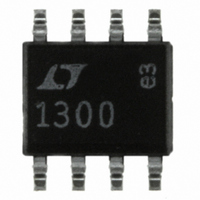
LT1300CS8 Linear Technology, LT1300CS8 Datasheet - Page 5

LT1300CS8
Manufacturer Part Number
LT1300CS8
Description
IC DC/DC CONV STP-UP HI-EFF8SOIC
Manufacturer
Linear Technology
Type
Step-Up (Boost)r
Datasheet
1.LT1300CN8PBF.pdf
(8 pages)
Specifications of LT1300CS8
Internal Switch(s)
Yes
Synchronous Rectifier
No
Number Of Outputs
1
Voltage - Output
3.3V, 5V
Current - Output
220mA
Frequency - Switching
155kHz
Voltage - Input
1.8 ~ 10 V
Operating Temperature
0°C ~ 70°C
Mounting Type
Surface Mount
Package / Case
8-SOIC (3.9mm Width)
Power - Output
500mW
Lead Free Status / RoHS Status
Contains lead / RoHS non-compliant
Available stocks
Company
Part Number
Manufacturer
Quantity
Price
Company:
Part Number:
LT1300CS8
Manufacturer:
LT
Quantity:
10 000
Part Number:
LT1300CS8
Manufacturer:
LT/凌特
Quantity:
20 000
Part Number:
LT1300CS8#PBF
Manufacturer:
LINEAR/凌特
Quantity:
20 000
Company:
Part Number:
LT1300CS8#TR
Manufacturer:
LinearTec
Quantity:
11 258
Company:
Part Number:
LT1300CS8#TRPBF
Manufacturer:
2002+
Quantity:
6 262
Part Number:
LT1300CS8#TRPBF
Manufacturer:
LINEAR/凌特
Quantity:
20 000
OPERATION
TEST CIRCUITS
Operation of the LT1300 is best understood by referring to
the Block Diagram in Figure 1. When A1’s negative input,
related to the Sense pin voltage by the appropriate resis-
tor-divider ratio, is higher that the 1.25V reference voltage,
A1’s output is low. A2, A3 and the oscillator are turned off,
drawing no current. Only the reference and A1 consume
current, typically 120 A. When the voltage at A1’s nega-
tive input decreases below 1.25V, overcoming A1’s 6mV
hysteresis, A1’s output goes high, enabling the oscillator,
current comparator A2, and driver A3. Quiescent current
increases to 2mA as the device prepares for high current
switching. Q1 then turns on in a controlled saturation for
(nominally) 5.3 s or until current comparator A2 trips,
whichever comes first. After a fixed off-time of (nominally)
1.2 s, Q1 turns on again. The LT1300’s switching causes
current to alternately build up in L1 and dump into capaci-
tor C2 via D1, increasing the output voltage. When the
output is high enough to cause A1’s output to go to low,
switching action ceases. C2 is left to supply current to the
load until V
high, and the entire cycle repeats.
If switch current reaches 1A, causing A2 to trip, switch on-
time is reduced and off-time increases slightly. This allows
continuous mode operation during bursts. Current com-
parator A2 monitors the voltage across 3 resistor R1
which is directly related to inductor L1’s current. Q2’s
collector current is set by the emitter-area ratio to 0.6%
of Q1’s collector current. When R1’s voltage drop exceeds
18mV, corresponding to 1A inductor current, A2’s output
goes high, truncating the on-time portion of the oscillator
cycle and increasing off-time to about 2 s as shown in
Figure 2, trace A. This programmed peak current can be
OUT
decreases enough to force A1’s output
U
2V
100µF
Oscillator Test Circuit
SEL
SENSE
GND
V
IN
LT1300
reduced by tying the I
flow through R2 into Q3’s collector. Q3’s current causes
a 10.4mV drop in R2 so that only an additional 7.6mV is
required across R1 to turn off the switch. This corre-
sponds to a 400mA switch current as shown in Figure 2,
trace B. The reduced peak switch current reduces I
loses in Q1, L1, C1 and D1. Efficiency can be increased by
doing this provided that the accompanying reduction in
full load output current is acceptable. Lower peak currents
also extend alkaline battery life due to the alkaline cell’s
high internal impedance. Typical operating waveforms are
shown in Figure 3.
AC COUPLED
PGND
SHDN
GROUNDED
500mA/DIV
500mA/DIV
Figure 2. Switch Pin Current With I
20mV/DIV
I
L
SW
TRACE A
TRACE B
I
I
5V/DIV
LIM
LIM
IA/DIV
OPEN
V
V
OUT
I
PIN
PIN
SW
SW
5V
Figure 3. Burst Mode Operation in Action
100
f
OUT
LIM
pin to ground, causing 15 A to
20 S/DIV
20 s/DIV
LIM
Floating or Grounded
LT1300
LT1300 F2
LT1300 F2
5
2
R


