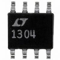
LT1304CS8-5#TR Linear Technology, LT1304CS8-5#TR Datasheet - Page 6

LT1304CS8-5#TR
Manufacturer Part Number
LT1304CS8-5#TR
Description
IC CONV DC/DC STEP UP 5V 8SOIC
Manufacturer
Linear Technology
Type
Step-Up (Boost)r
Datasheet
1.LT1304CS8-5PBF.pdf
(16 pages)
Specifications of LT1304CS8-5#TR
Internal Switch(s)
Yes
Synchronous Rectifier
No
Number Of Outputs
1
Voltage - Output
5V
Current - Output
200mA
Frequency - Switching
300kHz
Voltage - Input
1.5 ~ 8 V
Operating Temperature
0°C ~ 70°C
Mounting Type
Surface Mount
Package / Case
8-SOIC (3.9mm Width)
Power - Output
500mW
Lead Free Status / RoHS Status
Contains lead / RoHS non-compliant
Available stocks
Company
Part Number
Manufacturer
Quantity
Price
LT1304/LT1304-3.3/LT1304-5
OPERATIO
The LT1304’s operation can best be understood by exam-
ining the block diagram in Figure 1. Comparator A1
monitors the output voltage via resistor divider string
R3/R4 at the FB pin. When V
reference, A2 and the timers are turned off. Only the
reference, A1 and A3 consume current, typically 120 A.
As V
6mV), A1 enables the rest of the circuit. Power switch Q1
is then cycled on for 6 s, or until current comparator A2
turns off the ON timer, whichever comes first. Off-time is
fixed at approximately 1.5 s. Q1’s switching causes cur-
rent to alternately build up in inductor L1 and discharge
into output capacitor C2 via D1, increasing the output
voltage. As V
teresis, switching action ceases. C2 is left to supply
current to the load until V
A1’s output high, and the entire cycle repeats.
If switch current reaches 1A, causing A2 to trip, switch
ON time is reduced. This allows continuous mode opera-
tion during bursts. A2 monitors the voltage across 7.2
resistor R1, which is directly related to the switch current.
Q2’s collector current is set by the emitter-area ratio to
0.5% of Q1’s collector current. R1’s voltage drop exceeds
36mV, corresponding to 1A switch current, A2’s output
goes high, truncating the ON time part of the switch cycle.
The 1A peak current can be reduced by tying a resistor
between the I
to appear across R2. The drop offsets some of the 36mV
reference voltage, lowering peak current. A 22k resistor
limits current to approximately 550mA. A capacitor con-
nected between I
down is accomplished by grounding the SHDN pin.
The low-battery detector A3 has its own 1.17V reference
and is always on. The open collector output device can sink
up to 500 A. Approximately 35mV of hysteresis is built
into A3 to reduce “buzzing” as the battery voltage reaches
the trip level.
Inductor Selection
Inductors used with the LT1304 must be capable of
handling the worst-case peak switch current of 1.2A
without saturating. Open flux rod or drum core units may
be biased into saturation by 20% with only a small reduc-
6
FB
drops below 1.24V plus A1’s hysteresis (about
FB
LIM
increases enough to overcome C1’s hys-
LIM
pin and ground, causing a voltage drop
U
and ground provides soft start. Shut-
OUT
FB
decreases enough to force
is higher than the 1.24V
tion in efficiency. For the majority of 2-cell or 3-cell input
LT1304 applications, a 22 H or 20 H inductor such as the
Sumida CD54-220 (drum) or Coiltronics CTX20-1 (toroid)
will suffice. If switch current is reduced using the I
smaller inductors such as the Sumida CD43 series or
Coilcraft DO1608 series can be used. Minimizing DCR is
important for best efficiency. Ideally, the inductor DCR
should be less than 0.05 , although the physical size of
such an inductor makes its use prohibitive in many space
conscious applications. If EMI is a concern, such as when
sensitive analog circuitry is present, a toroidal inductor
such as the Coiltronics CTX20-1 is suggested.
A special case exists where the V
high, such as a 2V to 12V boost converter. If the required
duty cycle for continuous mode operation is higher than
the LT1304 can provide, the converter must be designed
for discontinuous operation. This means that the inductor
current decreases to zero during the switch OFF time. For
a simple step-up (boost) converter, duty cycle can be
calculated by the following formula:
where,
V
V
V
V
If the calculated duty cycle exceeds the minimum LT1304
duty cycle of 76%, the converter should be designed for
discontinuous mode operation. The inductance must be
low enough so that current in the inductor reaches the
peak current in a single cycle. Inductor value can be
calculated by:
where,
t
One advantage of discontinuous mode operation is that
inductor values are usually quite low so very small units
can be used. Ripple current is higher than with continuous
mode designs and efficiency will be somewhat less.
ON
IN
SAT
OUT
D
DC = 1 – [(V
L = (V
= Diode forward voltage (0.4V)
= Minimum input voltage
= Minimum on-time of LT1304 (4 s)
= Switch saturation voltage (0.3V)
= Output voltage
IN
– V
SAT
IN
– V
)(t
ON
SAT
/1A)
)/(V
OUT
+ V
OUT
D
)]
/V
IN
differential is
LIM
pin,


