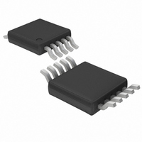
LTC1871EMS-7 Linear Technology, LTC1871EMS-7 Datasheet - Page 11

LTC1871EMS-7
Manufacturer Part Number
LTC1871EMS-7
Description
IC MULTI CONFIG SYNC ADJ 10MSOP
Manufacturer
Linear Technology
Type
Step-Up (Boost), Flyback, Sepicr
Datasheet
1.LTC1871EMS-7.pdf
(32 pages)
Specifications of LTC1871EMS-7
Internal Switch(s)
No
Synchronous Rectifier
No
Number Of Outputs
1
Voltage - Output
1.23 ~ 36 V
Current - Output
50mA
Frequency - Switching
50kHz ~ 1MHz
Voltage - Input
6 ~ 36 V
Operating Temperature
-40°C ~ 85°C
Mounting Type
Surface Mount
Package / Case
10-MSOP, Micro10™, 10-uMAX, 10-uSOP
Lead Free Status / RoHS Status
Contains lead / RoHS non-compliant
Power - Output
-
Available stocks
Company
Part Number
Manufacturer
Quantity
Price
Company:
Part Number:
LTC1871EMS-7
Manufacturer:
LT
Quantity:
10 000
OPERATION
can cause the LTC1871-7 to exceed its maximum junc-
tion temperature rating. The junction temperature can be
estimated using the following equations:
The total quiescent current I
supply current (I
discharge the gate of the power MOSFET. The 10-pin MSOP
package has a thermal resistance of R
As an example, consider a power supply with V
The switching frequency is 200kHz, and the maximum
ambient temperature is 70°C. The power MOSFET chosen
is the FDS3670(Fairchild), which has a maximum R
of 35mΩ (at room temperature) and a maximum total
gate charge of 80nC (the temperature coeffi cient of the
gate charge is low).
I
P
T
I
P
T
T
Q(TOT)
Q(TOT)
J
J
JRISE
IC
IC
= T
= 70°C + 120°C/W • 166mW = 89.9°C
= V
= 10V • 16.6mA = 166mW
A
= 19.9°C
IN
≈ I
= 600μA + 80nC • 200kHz = 16.6mA
+ P
• (I
Q
IC
+ f • Q
Q
• R
Q
+ f • Q
) and the current required to charge and
TH(JA)
G
G
1.230V
)
R2
Q(TOT)
Figure 7. Bypassing the LDO Regulator and Gate Driver Supply
–
+
LOGIC
consists of the static
TH(JA)
R1
= 120°C/W.
DRIVER
IN
DS(ON)
=10V.
P-CH
7V
INTV
GATE
GND
V
CC
IN
This demonstrates how signifi cant the gate charge current
can be when compared to the static quiescent current in
the IC.
To prevent the maximum junction temperature from being
exceeded, the input supply current must be checked when
operating in a continuous mode at high V
between the operating frequency and the size of the power
MOSFET may need to be made in order to maintain a reliable
IC junction temperature. Prior to lowering the operating
frequency, however, be sure to check with power MOSFET
manufacturers for their latest-and-greatest low Q
R
nologies are continually improving, with newer and better
performance devices being introduced almost yearly.
Output Voltage Programming
The output voltage is set by a resistor divider according
to the following formula:
The external resistor divider is connected to the output
as shown in Figure 1, allowing remote voltage sensing.
DS(ON)
18717 F07
V
O
= 1.230V • 1+
C
4.7μF
X5R
devices. Power MOSFET manufacturing tech-
VCC
PLACE AS CLOSE AS
POSSIBLE TO DEVICE PINS
C
IN
M1
R2
R1
INPUT
SUPPLY
6V TO 30V
GND
6V-RATED
POWER
MOSFET
LTC1871-7
IN
. A tradeoff
11
G
, low
18717fc


