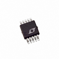
LT3758EMSE#PBF Linear Technology, LT3758EMSE#PBF Datasheet - Page 23

LT3758EMSE#PBF
Manufacturer Part Number
LT3758EMSE#PBF
Description
IC CTRLR DC/DC ADJ 10-MSOP
Manufacturer
Linear Technology
Type
Step-Up (Boost), Inverting, Flyback, Sepicr
Datasheet
1.LT3758EMSEPBF.pdf
(36 pages)
Specifications of LT3758EMSE#PBF
Internal Switch(s)
No
Synchronous Rectifier
No
Number Of Outputs
1
Frequency - Switching
100kHz ~ 1MHz
Voltage - Input
5.5 ~ 100 V
Operating Temperature
-40°C ~ 125°C
Mounting Type
Surface Mount
Package / Case
10-MSOP Exposed Pad, 10-HMSOP, 10-eMSOP
Dc To Dc Converter Type
FLYBACK CONTROLLER
Pin Count
10
Input Voltage
5.5 to 100V
Output Voltage
1.6 to 100V
Package Type
MSOP EP
Mounting
Surface Mount
Operating Temperature Classification
Automotive
Operating Temperature (min)
-40C
Operating Temperature (max)
125C
Lead Free Status / RoHS Status
Lead free / RoHS Compliant
Current - Output
-
Voltage - Output
-
Power - Output
-
Lead Free Status / Rohs Status
Compliant
Available stocks
Company
Part Number
Manufacturer
Quantity
Price
APPLICATIONS INFORMATION
MOSFET, its junction temperature can be obtained using
the following equation:
T
temperature rating. It is recommended to measure the
MOSFET temperature in steady state to ensure that absolute
maximum ratings are not exceeded.
SEPIC Converter: Output Diode Selection
To maximize effi ciency, a fast switching diode with a low
forward drop and low reverse leakage is desirable. The
average forward current in normal operation is equal to
the output current, and the peak current is equal to:
It is recommended that the peak repetitive reverse voltage
rating V
margin (a 10V safety margin is usually suffi cient).
The power dissipated by the diode is:
and the diode junction temperature is:
The R
for the device, plus the thermal resistance from the board,
to the ambient temperature in the enclosure. T
exceed the diode maximum junction temperature rating.
SEPIC Converter: Output and Input Capacitor Selection
The selections of the output and input capacitors of the
SEPIC converter are similar to those of the boost converter.
Please refer to the Boost Converter: Output Capacitor
Selection and Boost Converter: Input Capacitor Selection
sections.
SEPIC Converter: Selecting the DC Coupling Capacitor
The DC voltage rating of the DC coupling capacitor (C
as shown in Figure 1) should be larger than the maximum
input voltage:
J
T
P
T
V
I
must not exceed the MOSFET maximum junction
D PEAK
J
J
D
CDC
(
= T
= T
θJA
= I
RRM
> V
A
O(MAX)
A
used in this equation normally includes the R
)
+ P
+ P
=
IN(MAX)
is higher than V
⎛
⎝ ⎜
FET
D
1
• R
+
• V
• θ
χ
2
D
θJA
⎞
⎠ ⎟
JA
•
I
= T
O MAX
(
A
+ P
)
OUT
•
FET
1
−
+ V
• (θ
D
1
MAX
IN(MAX)
JC
+ θ
CA
by a safety
J
)
must not
θJC
DC
,
C
the switch off-time, the current through C
approximately –I
rating of the coupling capacitor is determined by the fol-
lowing equation:
A low ESR and ESL, X5R or X7R ceramic capacitor works
well for C
INVERTING CONVERTER APPLICATIONS
The LT3758 can be confi gured as a dual-inductor inverting
topology, as shown in Figure 10. The V
is:
in continuous conduction mode (CCM).
Inverting Converter: Switch Duty Cycle and Frequency
For an inverting converter operating in CCM, the duty cycle
of the main switch can be calculated based on the negative
output voltage (V
The maximum duty cycle (D
has the minimum input voltage:
DC
I
D
V
RMS CDC
has nearly a rectangular current waveform. During
MAX
OUT
V
(
V
IN
IN
−
=
DC
Figure 10. A Simplifi ed Inverting Converter
V
V
)
.
D
+
OUT
>
= −
LT3758
I
O MAX
C
SENSE
(
V
−
IN
GATE
O
OUT
GND
− 1
OUT
V
fl ows during the on-time. The RMS
D
L1
D
) and the input voltage (V
D
)
−
−
•
V
V
IN MIN
D
V
M1
MAX
R
+ –
(
V
OUT
C
SENSE
DC
IN MIN
) occurs when the converter
(
)
+
D1
V
)
D
L2
C
OUT
+
OUT
DC
LT3758
–
+
3758 F10
V
OUT
is I
to V
IN
IN
).
23
IN
, while
ratio
3758fb


