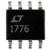
LT1776CS8#TR Linear Technology, LT1776CS8#TR Datasheet - Page 18

LT1776CS8#TR
Manufacturer Part Number
LT1776CS8#TR
Description
IC REG SW STEPDOWN HI EFF 8SOIC
Manufacturer
Linear Technology
Type
Step-Down (Buck)r
Datasheet
1.LT1776CS8PBF.pdf
(20 pages)
Specifications of LT1776CS8#TR
Internal Switch(s)
Yes
Synchronous Rectifier
No
Number Of Outputs
1
Voltage - Output
1.24 ~ 34 V
Current - Output
700mA
Frequency - Switching
200kHz
Voltage - Input
7.4 ~ 40 V
Operating Temperature
0°C ~ 125°C
Mounting Type
Surface Mount
Package / Case
8-SOIC (3.9mm Width)
Lead Free Status / RoHS Status
Contains lead / RoHS non-compliant
Power - Output
-
Available stocks
Company
Part Number
Manufacturer
Quantity
Price
LT1776
Figure 7b shows that efficiency is typically maintained at
75% or better down to a load current of 10mA. Even at a
load of 1mA, efficiency is still a respectable 58% to 68%,
depending on V
Resistor divider R1/R2 is still present, but does not
directly influence output voltage. It is chosen to ensure
that the LT1776 delivers high output current throughout
the voltage regulation range. Its presence is also required
to maintain proper short-circuit protection. Transistors
Q1, Q2 and resistor R7 form a high V
current voltage regulator to power U2.
Wide V
The circuit on the final page of this data sheet shows the
LT1776 configured as a constant-current/constant-volt-
age battery charger. An LT1620 rail-to-rail, current sense
amplifier (U2) monitors the differential voltage across
current sense resistor R4. As this equals and exceeds the
voltage set across resistor R5 in the R5/R6 divider, the
LT1620 responds by sinking current at its I
connected to the V
therefore acts to reduce the amount of power delivered to
the load. The overall constant-current/constant-voltage
behavior can be seen in the graph titled Battery Charger
Output Voltage vs Output Current.
Target voltage and current limits are independently pro-
grammable. Output voltage, presently 6V, is set by the
R1/R2 divider and the internal reference of the LT1776.
Output current, presently 200mA, is set by current sense
resistor R4 and the R5-R6 divider.
The circuit, as shown, accommodates an input voltage
range of 10V to 30V. The accompanying graphs display
efficiency for input voltages of 12V and 24V. The upper
input voltage limit of 30V is determined not by the LT1776,
but by the LT1121-5 regulator (U3). (A regulated 5V is
required by the LT1620.) This regulator was chosen for its
TYPICAL APPLICATIONS
18
IN
Range, High Efficiency Battery Charger
IN
.
C
control node of the LT1776 and
U
IN
, low quiescent
OUT
pin. This is
micropower behavior, which helps maintain good overall
efficiency. However, the basic catalog part is only rated to
30V. Substitution of the industry standard LM317, for
example, extends the allowable input voltage to 40V (or
more with the HV part), but its greater quiescent current
drain degrades efficiency from that shown.
A related concern in charger applications is the current
drain seen at the battery when charger power is removed.
Strictly speaking, this can occur in three separate ways:
the V
supply can be disconnected (V
SHDN function can be asserted. The worst-case is gener-
ally V
A diode is then required in the battery charger power path
to prevent reverse current flow. There are three logical
places for this diode. The first is directly in series with the
V
penalty, as the diode forward drop subtracts from the
input voltage. A disadvantage is that the battery must still
power the LT1776 V
several mA. In this position the diode is called upon to
switch on and off rapidly, so a Schottky type, similar to that
used as the freewheeling diode (D1), is recommended.
Placing the diode between output filter capacitor C2 and
feedback divider R1/R2 limits the current drain to only the
current drawn by the feedback divider, perhaps 100 A or
so. However, the efficiency penalty is greater, as the diode
forward drop is now in series with the output voltage.
When absolute minimal battery drain is required, the diode
may be placed between the R1/R2 feedback divider and
the battery itself. This limits current drain to just the
reverse leakage of the diode. In this case the feedback
divider must be adjusted for the nominal forward drop of
the diode. In either of these positions, a Schottky diode will
offer the least efficiency penalty, but a standard silicon
diode can be used in the most cost sensitive applications.
SW
node. This has the advantage of smallest efficiency
IN
IN
supply can go to zero (V
= 0V, and this situation will be assumed.
CC
pin, yielding a current drain of
IN
IN
= short circuit), the V
= open circuit) or the
IN


