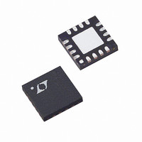
LTC3527EUD-1#PBF Linear Technology, LTC3527EUD-1#PBF Datasheet

LTC3527EUD-1#PBF
Specifications of LTC3527EUD-1#PBF
Available stocks
Related parts for LTC3527EUD-1#PBF
LTC3527EUD-1#PBF Summary of contents
Page 1
... The LTC3527-1 actively discharges OUT1 escent current in shutdown is less than 2μA. L, LT, LTC, LTM, Linear Technology and the Linear logo are registered trademarks and ThinSOT is a trademark of Linear Technology Corporation. All other trademarks are the property of their respective owners. 4.7μH V ...
Page 2
... Operating Temperature (Notes 2, 5) .........–40°C to 85°C Junction Temperature ........................................... 125°C Storage Temperature Range ...................–65°C to 125°C ORDER INFORMATION LEAD FREE FINISH TAPE AND REEL LTC3527EUD#PBF LTC3527EUD#TRPBF LTC3527EUD-1#PBF LTC3527EUD-1#TRPBF LEAD BASED FINISH TAPE AND REEL LTC3527EUD LTC3527EUD#TR LTC3527EUD-1 LTC3527EUD-1#TR Consult LTC Marketing for parts specifi ...
Page 3
ELECTRICAL CHARACTERISTICS temperature range, – ° ° IN PARAMETER PMOS Switch Leakage Current (LTC3527) NMOS and PMOS Combined Switch Leakage Current (LTC3527-1) NMOS Switch On-Resistance, SW1 NMOS Switch On-Resistance, SW2 PMOS Switch On-Resistance, ...
Page 4
LTC3527/LTC3527-1 TYPICAL PERFORMANCE CHARACTERISTICS Effi ciency vs Load Current and V IN for V = 1.8V at 1.2MHz OUT1 100 1.2V 1.5V 90 BURST 1. 1.5V 70 FIXED 0.01 0 ...
Page 5
TYPICAL PERFORMANCE CHARACTERISTICS No-Load Input Current 180 1.2MHz 160 140 OUT 120 100 3.3V OUT OUT OUT 2.4V 1.8V 0 0.5 1 1.5 2 ...
Page 6
LTC3527/LTC3527-1 TYPICAL PERFORMANCE CHARACTERISTICS Current Limit vs Temperature 1.30 CONVERTER1 1.20 1. 1. 3.3V OUT 0.90 0.80 0.70 CONVERTER2 0.60 0. –45 –30 – TEMPERATURE (°C) 35271 G17 ...
Page 7
TYPICAL PERFORMANCE CHARACTERISTICS V and I During Start-Up OUT IN V OUT1 1V/DIV INPUT CURRENT 200mA/DIV SHDN1 PIN 1V/DIV 100μs/DIV V = 3.3V OUT1 C = 10μF OUT1 V Load Step Response OUT1 Burst Mode Operation at 1.2MHz V OUT1 ...
Page 8
LTC3527/LTC3527-1 PIN FUNCTIONS SHDN1 (Pin 1): Boost Converter 1 Logic-Controlled Shutdown Input. There is an internal 4MΩ pull-down on this pin. • SHDN1 = High: Normal free running operation, 1.2MHz/ 2.2MHz typical operating frequency. • SHDN1 = Low: Shutdown, quiescent ...
Page 9
BLOCK DIAGRAM SW1 6 L1 4.7μ IN1 0.88V 4.7μF SHDN1 1 PGOOD1 FSEL 10 3 MODE V REF_GD SW2 7 L2 4.7μH V IN2 9 SHDN2 12 PGOOD2 ...
Page 10
LTC3527/LTC3527-1 OPERATION (Refer to Block Diagram) The LTC3527/LTC3527-1 are dual 1.2MHz/2.2MHz syn- chronous boost converters housed in a 16-lead 3mm × 3mm QFN package. With the ability to start up and operate from inputs less than 880mV, these devices feature ...
Page 11
OPERATION to FB1 for converter 1 and FB2 for converter 2. Clamps limit the minimum and maximum error amp output volt- ages for improved large-signal transient response. Power converter control loop compensation is provided internally. An external resistive voltage divider ...
Page 12
LTC3527/LTC3527-1 OPERATION output until it reaches the nominal regulation value, then the LTC3527/LTC3527-1 transition to sleep mode where the outputs are off and the LTC3527/LTC3527-1 consume only 12μA of quiescent current from the higher When the ...
Page 13
APPLICATIONS INFORMATION PCB Layout Guidelines The high speed operation of the LTC3527/LTC3527-1 demands careful attention to board layout. A careless layout will result in reduced performance. Figure 1 shows the recommended component placement. A large ground pin copper area will ...
Page 14
LTC3527/LTC3527-1 APPLICATIONS INFORMATION Table 1. Recommended Inductors VENDOR PART/STYLE Coilcraft MSS5131 www.coilcraft.com MSS4020 ME3220 Coiltronics SD10 www.cooperet.com SD12 FDK MIP3226D www.fdk.com MIPF2520D Murata LQH43C www.murata.com LQH32C Sumida CDRH3D16 www.sumida.com CDRH2D14 TDK VLF3010A www.global.tdk.co.jp VLF5012A Taiyo Yuden NR3010 www.t-yuden.com NR3015 Output ...
Page 15
TYPICAL APPLICATIONS 0.85V TO 1.60V + SINGLE ALKALINE CELL V OUT 3V C 150mA 4.7μF ON OFF ON OFF L: SUMIDA CDRH3D164R7 TAIYO YUDEN X5R JMK212BJ475MD IN OUT Boost 1 Effi ciency 100 1.2V 1.5V 90 ...
Page 16
LTC3527/LTC3527-1 TYPICAL APPLICATIONS 0.85V TO 1.60V + SINGLE ALKALINE CELL V OUT 1.8V C 200mA OUT1 4.7μF ON OFF ON OFF L: SUMIDA CDRH3D164R7 TAIYO YUDEN X5R JMK212BJ475MD IN OUT Boost 1 Effi ciency 100 1.2V ...
Page 17
TYPICAL APPLICATIONS 0.85V TO 1.60V + SINGLE ALKALINE CELL V OUT 3.3V C 150mA OUT1 4.7μF ON OFF ON OFF L: SUMIDA CDRH3D162R2 TAIYO YUDEN X5R JMK212BJ475MD IN OUT Boost 1 Effi ciency 100 1.2V 1.5V ...
Page 18
LTC3527/LTC3527-1 TYPICAL APPLICATIONS 1.8V TO 3.2V + ALKALINE + CELLS V OUT 5V 300mA C OUT1 4.7μF ON OFF ON OFF L: SUMIDA CDRH3D164R7 TAIYO YUDEN X5R JMK212BJ475MD IN OUT Boost 1 Effi ciency 100 2.4V ...
Page 19
TYPICAL APPLICATIONS 0.85V TO 1.60V + SINGLE ALKALINE CELL V OUT 1.8V 200mA ON OFF L: SUMIDA CDRH3D164R7 OUT Boost 1 Effi ciency 100 1.2V 1.5V 90 BURST FIXED ...
Page 20
LTC3527/LTC3527-1 PACKAGE DESCRIPTION 3.50 ± 0.05 1.45 ± 0.05 2.10 ± 0.05 (4 SIDES) RECOMMENDED SOLDER PAD PITCH AND DIMENSIONS 3.00 ± 0.10 (4 SIDES) PIN 1 TOP MARK (NOTE 6) NOTE: 1. DRAWING CONFORMS TO JEDEC PACKAGE OUTLINE MO-220 ...
Page 21
... Change to Operation Section Changes to Applications Information Section Information furnished by Linear Technology Corporation is believed to be accurate and reliable. However, no responsibility is assumed for its use. Linear Technology Corporation makes no representa- tion that the interconnection of its circuits as described herein will not infringe on existing patent rights. LTC3527/LTC3527-1 ...
Page 22
... OUT(MAX 6V 12μA, DFN-12 Package OUT(MAX ) Q = 10V 10μA, I < 1μA, OUT(MAX 0.85V to 5V 5.25V 7μA, IN OUT(MAX 0.85V to 5V 5.25V 10μA/300μA, IN OUT(MAX 0.85V to 5V 5.25V 10μA/300μA, IN OUT(MAX 1109 REV C • PRINTED IN USA © LINEAR TECHNOLOGY CORPORATION 2007 < 1μA, 35271fc ...


