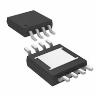
LT1767EMS8E Linear Technology, LT1767EMS8E Datasheet - Page 3

LT1767EMS8E
Manufacturer Part Number
LT1767EMS8E
Description
IC SW REG STEP-DOWN 1.5A 8-MSOP
Manufacturer
Linear Technology
Type
Step-Down (Buck)r
Datasheet
1.LT1767EMS8-3.3PBF.pdf
(16 pages)
Specifications of LT1767EMS8E
Internal Switch(s)
Yes
Synchronous Rectifier
No
Number Of Outputs
1
Voltage - Output
1.2 ~ 20 V
Current - Output
1.5A
Frequency - Switching
1.25MHz
Voltage - Input
3 ~ 25 V
Operating Temperature
-40°C ~ 125°C
Mounting Type
Surface Mount
Package / Case
8-MSOP Exposed Pad, 8-HMSOP, 8-eMSOP
Lead Free Status / RoHS Status
Contains lead / RoHS non-compliant
Power - Output
-
Available stocks
Company
Part Number
Manufacturer
Quantity
Price
Company:
Part Number:
LT1767EMS8E
Manufacturer:
LT
Quantity:
5 321
Company:
Part Number:
LT1767EMS8E
Manufacturer:
Linear Technology
Quantity:
1 827
Company:
Part Number:
LT1767EMS8E
Manufacturer:
LT
Quantity:
10 000
Part Number:
LT1767EMS8E
Manufacturer:
LT
Quantity:
20 000
Company:
Part Number:
LT1767EMS8E#PBF
Manufacturer:
LT
Quantity:
7 500
Part Number:
LT1767EMS8E#PBF
Manufacturer:
LT/凌特
Quantity:
20 000
Company:
Part Number:
LT1767EMS8E#TRA1PB
Manufacturer:
MX
Quantity:
249
Part Number:
LT1767EMS8E#TRPBF
Manufacturer:
LINEAR/凌特
Quantity:
20 000
Part Number:
LT1767EMS8E-1.8
Manufacturer:
LINEAR/凌特
Quantity:
20 000
Part Number:
LT1767EMS8E-1.8#TRPBF
Manufacturer:
LINEAR/凌特
Quantity:
20 000
ELECTRICAL CHARACTERISTICS
The
V
PARAMETER
FB Input Resistance
Error Amp Voltage Gain
Error Amp Transconductance
V
V
V
V
V
Maximum Switch Duty Cycle
Minimum Boost Voltage Above Switch
Boost Current
SHDN Threshold Voltage
SHDN Input Current (Shutting Down)
SHDN Threshold Current Hysteresis
SYNC Threshold Voltage
SYNC Input Frequency
SYNC Pin Resistance
Note 1: Absolute Maximum Ratings are those values beyond which the life
of a device may be impaired.
Note 2: The LT1767E is guaranteed to meet performance specifications
from 0 C to 125 C. Specifications over the – 40 C to 125 C operating
junction temperature range are assured by design, characterization and
correlation with statistical process controls.
TYPICAL PERFORMANCE CHARACTERISTICS
C
C
C
C
C
IN
Pin Source Current
Pin Sink Current
Pin to Switch Current Transconductance
Pin 1.5A I
Pin Minimum Switching Threshold
1.22
1.21
1.20
1.19
1.18
= 15V, V
–50
denotes the specifications which apply over the full operating temperature range, otherwise specifications are at T
FB vs Temperature (Adj)
–25
SW
C
= 0.8V, Boost = V
Threshold
0
TEMPERATURE ( C)
25
50
IN
75
W
+ 5V, SHDN, SYNC and switch open unless otherwise noted.
100
U
1767 G01
CONDITION
LT1767-1.8
LT1767-2.5
LT1767-3.3
LT1767-5
0.4V < V
V
V
Duty Cycle = 0%
V
I
I
I
SHDN = 60mV Above Threshold
SHDN = 100mV Below Threshold
I
125
SW
SW
SW
SYNC
FB
FB
C
I
VC
= 1.2V, I
= V
= V
= –1.5A, 0 C T
= – 0.5A (Note 4)
= –1.5A, 0 C T
= 10 A
= 1mA
NOM
NOM
C
400
350
300
250
200
150
100
< 0.9V
50
SW
– 17%
+ 17%
0
0
Switch On Voltage Drop
= 400mA
A
A
SWITCH CURRENT (A)
125 C and –1.3A, T
125 C and –1.3A, T
0.5
LT1767-2.5/LT1767-3.3/LT1767-5
Note 3: Minimum input voltage is defined as the voltage where the internal
regulator enters lockout. Actual minimum input voltage to maintain a
regulated output will depend on output voltage and load current. See
Applications Information.
Note 4: Current flows into the BOOST pin only during the on period of the
switch cycle.
1
125 C
–40 C
A
A
25 C
< 0 C
< 0 C (Note 4)
1767 G02
1.5
LT1767/LT1767-1.8/
1.50
1.45
1.40
1.35
1.30
1.25
1.20
1.15
1.10
–50
Oscillator Frequency
10.5
14.7
1.27
MIN
150
500
1.5
–25
19
29
80
70
85
80
– 7
4
0
TEMPERATURE ( C)
27.5
0.35
1.33
TYP
–10
350
850
120
110
2.5
0.9
1.8
1.5
15
21
42
90
10
30
20
7
25
50
MAX
1300
1.40
160
180
–13
2.7
2.2
A
21
30
39
60
15
45
10
2
75
= 25 C.
sn1767 1767fas
100
UNITS
1767 G03
3
Mho
MHz
A/V
mA
mA
k
k
k
k
k
125
%
%
A
A
V
V
V
V
A
A
V


