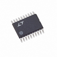
LTC1735CF#TRPBF Linear Technology, LTC1735CF#TRPBF Datasheet - Page 7

LTC1735CF#TRPBF
Manufacturer Part Number
LTC1735CF#TRPBF
Description
IC SW REG SYNC STEP-DWN 20-TSSOP
Manufacturer
Linear Technology
Type
Step-Down (Buck)r
Datasheet
1.LTC1735CSPBF.pdf
(32 pages)
Specifications of LTC1735CF#TRPBF
Internal Switch(s)
No
Synchronous Rectifier
Yes
Number Of Outputs
1
Voltage - Output
0.8 ~ 6 V
Current - Output
3A
Frequency - Switching
300kHz
Voltage - Input
4 ~ 30 V
Operating Temperature
0°C ~ 85°C
Mounting Type
Surface Mount
Package / Case
20-TSSOP
Lead Free Status / RoHS Status
Lead free / RoHS Compliant
Power - Output
-
Available stocks
Company
Part Number
Manufacturer
Quantity
Price
C
the operating frequency.
RUN/SS: Combination of Soft-Start and Run Control In-
puts. A capacitor to ground at this pin sets the ramp time
to full output current. The time is approximately 1.25s/ F.
Forcing this pin below 1.5V causes the device to shut
down. (See Applications Information section for quiescent
current note.) In shutdown all functions, including INTV
are disabled. Latchoff overcurrent protection is also in-
voked via this pin as described in the Applications Infor-
mation section.
I
comparator threshold increases with this control voltage.
Nominal voltage range for this pin is 0V to 2.4V.
TYPICAL PERFOR A CE CHARACTERISTICS
20mV/DIV
PI FU CTIO S
TH
V
OSC
1V/DIV
5V/DIV
5A/DIV
RUN/SS
5A/DIV
V
: Error Amplifier Compensation Point. The current
V
U
OUT
OUT
I
: External capacitor C
I
L
L
V
V
R
Start-Up
FCB = 5V
V
V
V
(Burst Mode Operation)
IN
OUT
LOAD
IN
OUT
I
OUT(RIPPLE)
LOAD
= 15V
= 15V
= 1.6V
= 1.6V
= 0.16
U
= 1.5A
5ms/DIV
5 s/DIV
U
OSC
W
from this pin to ground sets
FIGURE 1
U
1735 G22
1735 G27
50mV/DIV
10mV/DIV
5A/DIV
5A/DIV
V
V
OUT
OUT
I
I
L
L
10mA TO
9A LOAD STEP
FCB = 5V
V
V
V
EXT SYNC f = f
V
V
Load Step (Burst Mode Operation)
IN
OUT
IN
OUT
OUT(RIPPLE)
I
LOAD
= 15V
= 15V
= 1.6V
= 1.6V
= 10mA
CC
,
O
(Synchronized)
10 s/DIV
10 s/DIV
FCB: Forced Continuous/Synchronization Input. Tie this
pin to ground for continuous synchronous operation, to a
resistive divider from the secondary output when using a
secondary winding or to INTV
operation at low load currents. Clocking this pin with a
signal above 1.5V
allows cycle-skipping at low load currents and synchro-
nizes the internal oscillator with the external clock. The
FCB pin must not be driven when the device is shut down
(RUN/SS pin low).
SGND: Small-Signal Ground. All small-signal components
such as C
pensation resistor and capacitor(s) should single-point tie
to this pin. This pin should, in turn, connect to PGND.
FIGURE 1
FIGURE 1
OSC
, C
1735 G26
1735 G23
SS
, the feedback divider plus the loop com-
P–P
50mV/DIV
20mV/DIV
5A/DIV
disables Burst Mode operation but
5A/DIV
V
V
OUT
OUT
I
I
L
L
Load Step (Continuous Mode)
0A TO
9A LOAD STEP
FCB = 0V
V
V
V
(Burst Mode Operation)
FCB = 5V
V
V
IN
OUT
IN
OUT
OUT(RIPPLE)
I
LOAD
= 15V
= 15V
= 1.6V
= 1.6V
CC
= 50mA
to enable Burst Mode
10 s/DIV
50 s/DIV
LTC1735
FIGURE 1
FIGURE 1
1735fc
7
1735 G24
1735 G25


