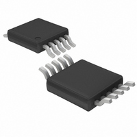
LTC1871IMS#TR Linear Technology, LTC1871IMS#TR Datasheet - Page 7

LTC1871IMS#TR
Manufacturer Part Number
LTC1871IMS#TR
Description
IC MULTI CONFIG SYNC ADJ 10MSOP
Manufacturer
Linear Technology
Type
Step-Up (Boost), Flyback, Sepicr
Datasheet
1.LTC1871EMS.pdf
(36 pages)
Specifications of LTC1871IMS#TR
Internal Switch(s)
No
Synchronous Rectifier
No
Number Of Outputs
1
Voltage - Output
1.23 ~ 72 V
Current - Output
50mA
Frequency - Switching
50kHz ~ 1MHz
Voltage - Input
2.5 ~ 36 V
Operating Temperature
-40°C ~ 125°C
Mounting Type
Surface Mount
Package / Case
10-MSOP, Micro10™, 10-uMAX, 10-uSOP
Lead Free Status / RoHS Status
Contains lead / RoHS non-compliant
Power - Output
-
Available stocks
Company
Part Number
Manufacturer
Quantity
Price
PIN FUNCTIONS
RUN (Pin 1): The RUN pin provides the user with an
accurate means for sensing the input voltage and pro-
gramming the start-up threshold for the converter. The
falling RUN pin threshold is nominally 1.248V and the
comparator has 100mV of hysteresis for noise immunity.
When the RUN pin is below this input threshold, the IC
is shut down and the V
value (typ 10μA). The Absolute Maximum Rating for the
voltage on this pin is 7V.
I
current comparator input threshold increases with this
control voltage. Nominal voltage range for this pin is 0V
to 1.40V.
FB (Pin 3): Receives the feedback voltage from the external
resistor divider across the output. Nominal voltage for
this pin in regulation is 1.230V.
FREQ (Pin 4): A resistor from the FREQ pin to ground
programs the operating frequency of the chip. The nominal
voltage at the FREQ pin is 0.6V.
MODE/SYNC (Pin 5): This input controls the operating
mode of the converter and allows for synchronizing the
TH
(Pin 2): Error Amplifi er Compensation Pin. The
IN
supply current is kept to a low
operating frequency to an external clock. If the MODE/
SYNC pin is connected to ground, Burst Mode operation
is enabled. If the MODE/SYNC pin is connected to INTV
or if an external logic-level synchronization signal is ap-
plied to this input, Burst Mode operation is disabled and
the IC operates in a continuous mode.
GND (Pin 6): Ground Pin.
GATE (Pin 7): Gate Driver Output.
INTV
The gate driver and control circuits are powered from
this voltage. Decouple this pin locally to the IC ground
with a minimum of 4.7μF low ESR tantalum or ceramic
capacitor.
V
to ground.
SENSE (Pin 10): The Current Sense Input for the Control
Loop. Connect this pin to the drain of the power MOSFET
for V
SENSE pin may be connected to a resistor in the source
of the power MOSFET. Internal leading edge blanking is
provided for both sensing methods.
IN
(Pin 9): Main Supply Pin. Must be closely decoupled
DS
CC
sensing and highest effi ciency. Alternatively, the
(Pin 8): The Internal 5.20V Regulator Output.
LTC1871
1871fe
7
CC
,


