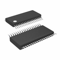
LTC3865IFE#PBF Linear Technology, LTC3865IFE#PBF Datasheet - Page 25

LTC3865IFE#PBF
Manufacturer Part Number
LTC3865IFE#PBF
Description
IC BUCK SYNC ADJ DUAL 38TSSOP
Manufacturer
Linear Technology
Type
Step-Down (Buck)r
Datasheet
1.LTC3865EUHPBF.pdf
(38 pages)
Specifications of LTC3865IFE#PBF
Internal Switch(s)
No
Synchronous Rectifier
Yes
Number Of Outputs
2
Voltage - Output
0.6 ~ 5 V
Frequency - Switching
250kHz ~ 770kHz
Voltage - Input
4.5 ~ 38 V
Operating Temperature
-40°C ~ 125°C
Mounting Type
Surface Mount
Package / Case
38-TSSOP Exposed Pad, 38-eTSSOP, 38-HTSSOP
Lead Free Status / RoHS Status
Lead free / RoHS Compliant
Current - Output
-
Power - Output
-
Available stocks
Company
Part Number
Manufacturer
Quantity
Price
APPLICATIONS INFORMATION
If the external clock frequency is greater than the inter-
nal oscillator’s frequency, f
continuously from the phase detector output, pulling up
the fi lter network. When the external clock frequency is
less than f
the fi lter network. If the external and internal frequencies
are the same but exhibit a phase difference, the current
sources turn on for an amount of time corresponding to
the phase difference. The voltage on the fi lter network is
adjusted until the phase and frequency of the internal and
external oscillators are identical. At the stable operating
point, the phase detector output is high impedance and
the fi lter capacitor holds the voltage.
Typically, the external clock (on MODE/PLLIN pin)
input high threshold is 1.6V, while the input low thres-hold
is 1V. The external clock should not be applied when the
IC is in shutdown.
Minimum On-Time Considerations
Minimum on-time, t
that the LTC3865/LTC3865-1 is capable of turning on the
top MOSFET. It is determined by internal timing delays
and the gate charge required to turn on the top MOSFET.
Low duty cycle applications may approach this minimum
on-time limit and care should be taken to ensure that
If the duty cycle falls below what can be accommodated
by the minimum on-time, the controller will begin to skip
cycles. The output voltage will continue to be regulated,
but the ripple voltage and current will increase.
The minimum on-time for the LTC3865/LTC3865-1 is
approximately 90ns, with reasonably good PCB layout,
minimum 30% inductor current ripple and at least 10mV
to 15mV ripple on the current sense signal. The mini-
mum on-time can be affected by PCB switching noise in
the voltage and current loop. As the peak sense voltage
t
ON MIN
(
OSC
)
<
, current is sunk continuously, pulling down
V
V
IN
OUT
( )
f
ON(MIN)
, is the smallest time duration
OSC
, then current is sourced
decreases the minimum on-time gradually increases to
130ns. This is of particular concern in forced continuous
applications with low ripple current at light loads. If the
duty cycle drops below the minimum on-time limit in this
situation, a signifi cant amount of cycle skipping can occur
with correspondingly larger current and voltage ripple.
Effi ciency Considerations
The percent effi ciency of a switching regulator is equal to
the output power divided by the input power times 100%.
It is often useful to analyze individual losses to determine
what is limiting the effi ciency and which change would
produce the most improvement. Percent effi ciency can
be expressed as:
where L1, L2, etc. are the individual losses as a percent-
age of input power.
Although all dissipative elements in the circuit produce
losses, four main sources usually account for most of the
losses in LTC3865/LTC3865-1 circuits: 1) IC V
2) INTV
MOSFET transition losses.
1. The V
2. INTV
%Effi ciency = 100% – (L1 + L2 + L3 + ...)
the Electrical Characteristics table, which excludes
MOSFET driver and control currents. V
cally results in a small (<0.1%) loss.
control currents. The MOSFET driver current results
from switching the gate capacitance of the power
MOSFETs. Each time a MOSFET gate is switched from
low to high to low again, a packet of charge dQ moves
from INTV
rent out of INTV
control circuit current. In continuous mode, I
= f(Q
the topside and bottom side MOSFETs.
CC
T
CC
IN
+ Q
current is the sum of the MOSFET driver and
regulator current, 3) I
current is the DC supply current given in
B
CC
), where Q
LTC3865/LTC3865-1
to ground. The resulting dQ/dt is a cur-
CC
that is typically much larger than the
T
and Q
B
are the gate charges of
2
R losses, 4) Topside
IN
current typi-
IN
GATECHG
current,
25
3865fb


