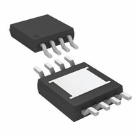
LT3663IMS8E-3.3#TRPBF Linear Technology, LT3663IMS8E-3.3#TRPBF Datasheet - Page 11

LT3663IMS8E-3.3#TRPBF
Manufacturer Part Number
LT3663IMS8E-3.3#TRPBF
Description
IC BUCK 3.3V 1.2A 8MSOP
Manufacturer
Linear Technology
Type
Step-Down (Buck)r
Datasheet
1.LT3663EDCBTRMPBF.pdf
(16 pages)
Specifications of LT3663IMS8E-3.3#TRPBF
Internal Switch(s)
Yes
Synchronous Rectifier
No
Number Of Outputs
1
Voltage - Output
3.3V
Current - Output
1.2A
Frequency - Switching
1MHz
Voltage - Input
7.5 ~ 36 V
Operating Temperature
-40°C ~ 125°C
Mounting Type
Surface Mount
Package / Case
8-MSOP Exposed Pad, 8-HMSOP, 8-eMSOP
Lead Free Status / RoHS Status
Lead free / RoHS Compliant
Power - Output
-
Available stocks
Company
Part Number
Manufacturer
Quantity
Price
Part Number:
LT3663IMS8E-3.3#TRPBFLT3663IMS8E-3.3
Manufacturer:
Linear Technology
Quantity:
135
APPLICATIONS INFORMATION
PCB Layout
Proper operation and minimum EMI, requires careful
printed circuit board layout. Figure 5 shows the recom-
mended component placement with trace, ground plane
and via locations. Note that large, switched currents fl ow
in the LT3663’s V
and the input capacitor (C1). Keep the loop formed by
these components as small as possible and tied to system
ground in only one place. Locate these components, along
with the inductor and output capacitor, on the same side
of the circuit board, and keep their connections on that
layer. Place a local, unbroken ground plane below these
components, and tie this ground plane to system ground
at one location, ideally at the ground terminal of the output
capacitor C1. Make the SW and BOOST PCB trace as short
as possible. Include vias near the exposed GND pad of
the LT3663 to help remove heat from the LT3663 to the
ground plane.
High Temperature Considerations
The die temperature of the LT3663 must not exceed the
maximum rating. This is generally not a concern unless
IN
and SW pins, the catch diode (D2)
V
RUN
IN
R1
R2
Figure 5. LT3663 PCB Layout
C1
4
1
2
3
R
ILIM
LT3663
GND
the ambient temperature is above 85°C. For higher tem-
peratures, take care in the layout of the circuit to ensure
good heat sinking of the LT3663. De-rate the maximum
load current as the ambient temperature approaches the
maximum temperature rating. Calculate the die tempera-
ture by multiplying the LT3663 power dissipation by the
thermal resistance from junction to ambient. Estimate
the power dissipation within the LT3663 by calculating
the total power loss from an effi ciency measurement
and subtracting the catch diode loss. Thermal resistance
depends on the layout of the circuit board, but 64°C/W is
typical for the (2mm × 3mm) DFN (DCB) package.
Other Linear Technology Publications
Application Notes 19, 35 and 44 contain more detailed
descriptions and design information for Buck regulators
and other switching regulators. The LT1376 data sheet
has a more extensive discussion of output ripple, loop
compensation and stability testing. Design Note 100
shows how to generate a bipolar output supply using a
Buck regulator.
C2
8
7
6
5
D1
C3
V
OUT
3663 F05
L
LT3663
11
3663fb


