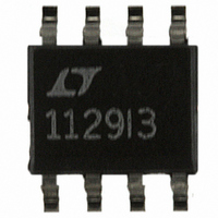
LT1107CS8 Linear Technology, LT1107CS8 Datasheet - Page 3

LT1107CS8
Manufacturer Part Number
LT1107CS8
Description
IC DC/DC CONV ADJUSTBL OUT 8SOIC
Manufacturer
Linear Technology
Type
Step-Down (Buck), Step-Up (Boost), Invertingr
Datasheet
1.LT1107CS8PBF.pdf
(16 pages)
Specifications of LT1107CS8
Internal Switch(s)
Yes
Synchronous Rectifier
No
Number Of Outputs
1
Voltage - Output
Adjustable
Current - Output
400mA
Frequency - Switching
63kHz
Voltage - Input
2 ~ 30 V
Operating Temperature
0°C ~ 70°C
Mounting Type
Surface Mount
Package / Case
8-SOIC (3.9mm Width)
Power - Output
500mW
Lead Free Status / RoHS Status
Contains lead / RoHS non-compliant
Available stocks
Company
Part Number
Manufacturer
Quantity
Price
Company:
Part Number:
LT1107CS8
Manufacturer:
LT
Quantity:
5 510
Part Number:
LT1107CS8
Manufacturer:
LINEAR/凌特
Quantity:
20 000
Part Number:
LT1107CS8#PBF
Manufacturer:
LINEAR/凌特
Quantity:
20 000
Part Number:
LT1107CS8#TRPBF
Manufacturer:
LINEAR/凌特
Quantity:
20 000
Part Number:
LT1107CS8-12
Manufacturer:
LINEAR/凌特
Quantity:
20 000
Part Number:
LT1107CS8-12#PBF
Manufacturer:
LINEAR/凌特
Quantity:
20 000
The
noted.
temperature range, V
SYMBOL
V
A
V
The
otherwise noted.
SYMBOL
I
f
DC
t
V
SYMBOL
I
f
DC
t
V
Note 1: Absolute Maximum Ratings are those values beyond which the life
of a device may be impaired.
Note 2: This specification guarantees that both the high and low trip points
of the comparator fall within the 1.2V to 1.3V range.
ELECTRICAL C
Q
OSC
ON
Q
OSC
ON
OL
V
SW2
SAT
SAT
denotes the specifications which apply over the full operating temperature range, V
denotes the specifications which apply over the full operating temperature range, V
PARAMETER
Feedback Pin Bias Current
Set Pin Bias Current
Gain Block Output Low
Reference Line Regulation
Gain Block Gain
Current Limit
Current Limit Temperature Coefficient
Switch OFF Leakage Current
Maximum Excursion Below GND
PARAMETER
Quiescent Current
Oscillator Frequency
Duty Cycle
Switch ON Time
Reference Line Regulation
Switch Saturation Voltage, Step-Up Mode
Switch Saturation Voltage, Step-Down Mode
PARAMETER
Quiescent Current
Oscillator Frequency
Duty Cycle
Switch ON Time
Reference Line Regulation
Switch Saturation Voltage, Step-Up Mode
Switch Saturation Voltage, Step-Down Mode
IN
= 3V, military or commercial version, T
HARA TERISTICS
C
Step-Up Mode
Step-Up Mode
CONDITIONS
LT1107, V
V
I
5V V
R
220 to I
Measured at SW1 Pin, V
I
CONDITIONS
Switch OFF
Step-Down Mode, V
Step-Up Mode
Step-Down Mode, V
2V V
2.4V V
0 C T
T
V
CONDITIONS
Switch OFF
Step-Down Mode, V
Step-Up Mode
Step-Down Mode, V
2V V
V
V
SINK
SW1
SET
A
IN
IN
IN
L
= – 55 C, I
= 100k (Note 4)
The
0 C T
T
= 12V, I
= 3V, I
= 12V, I
A
= V
= 300 A, V
IN
IN
= – 55 C
IN
10 A, Switch OFF
A
A
REF
IN
LIM
= 25 C, unless otherwise noted.
FB
SW
denotes the specifications which apply over the full operating
A
30V
5V, 0 C T
5V
125 C, I
SW
SW
= 0V
5V, T
to V
SW
= 650mA
125 C
= 500mA
= 650mA
Note 3: The output voltage waveform will exhibit a sawtooth shape due to
the comparator hysteresis. The output voltage on the fixed-output versions
will always be within the specified range.
Note 4: 100k resistor connected between a 5V source and the AO pin.
SET
= 400mA
IN
A
SW
IN
IN
IN
IN
= 1V
= – 55 C
= 12V
= 12V
= 12V
= 12V
A
= 500mA
SW1
125 C
= 12V
IN
IN
= 3V, 0 C T
= 3V, – 55 C T
1000
MIN
MIN
MIN
40
56
45
50
62
50
7
5
8
6
A
LT1107M
LT1107C
– 400
A
6000
– 0.3
70 C, unless otherwise
0.15
0.02
TYP
400
TYP
TYP
0.2
0.5
0.5
0.2
0.5
1.1
70
70
63
69
60
11
63
69
60
11
1
9
9
125 C, unless
0.075
– 350
MAX
MAX
MAX
0.65
0.65
13.5
12.0
0.65
120
300
500
450
0.4
0.4
0.8
1.5
2.0
0.7
1.5
10
95
81
73
15
13
88
78
70
LT1107
UNITS
UNITS
UNITS
1107fa
%/ C
3
%/V
%/V
%/V
%/V
V/V
kHz
kHz
mA
mV
nA
nA
%
%
%
%
V
A
A
V
V
V
V
A
V
V
s
s
s
s


