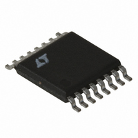
LT1940EFE#TR Linear Technology, LT1940EFE#TR Datasheet - Page 14

LT1940EFE#TR
Manufacturer Part Number
LT1940EFE#TR
Description
IC REG SW DUAL 1.4A STDN 16TSSOP
Manufacturer
Linear Technology
Type
Step-Down (Buck)r
Datasheet
1.LT1940EFEPBF.pdf
(20 pages)
Specifications of LT1940EFE#TR
Internal Switch(s)
Yes
Synchronous Rectifier
No
Number Of Outputs
2
Voltage - Output
1.25 ~ 22 V
Current - Output
1.4A
Frequency - Switching
1.1MHz
Voltage - Input
3.6 ~ 25 V
Operating Temperature
-40°C ~ 85°C
Mounting Type
Surface Mount
Package / Case
16-TSSOP Exposed Pad, 16-eTSSOP, 16-HTSSOP
Lead Free Status / RoHS Status
Contains lead / RoHS non-compliant
Power - Output
-
Available stocks
Company
Part Number
Manufacturer
Quantity
Price
LT1940/LT1940L
APPLICATIO S I FOR ATIO
Shorted Input Protection
If the inductor is chosen so that it won’t saturate exces-
sively, the LT1940 will tolerate a shorted output. There is
another situation to consider in systems where the output
will be held high when the input to the LT1940 is absent.
If the V
then the LT1940’s internal circuitry will pull its quiescent
current through its SW pin. This is fine if your system can
tolerate a few mA of load in this state. With both RUN/SS
pins grounded, the LT1940 enters shutdown mode and
the SW pin current drops to ~30 A. However, if the V
is grounded while the output is held high, then parasitic
diodes inside the LT1940 can pull large currents from the
output through the SW pin and the V
diode in series with the input to the LT1940 will protect the
LT1940 and the system from a shorted or reversed input.
14
IN
OFF2 ON2
and one of the RUN/SS pins are allowed to float,
OFF
OFF
Figure 6. Diode D4 Prevents a Shorted Input from Discharging a Backup Battery Tied to the Output.
ON
ON
U
Figure 5. Several Methods of Sequencing the Two Outputs. Channel 1 Starts First.
U
(5c) Independent Control of Channel 2
(5a) Channel 2 is Delayed
2.2nF
1.5nF
W
1nF
1nF
IN
V
RUN/SS1
RUN/SS2
RUN/SS1
PG1
RUN/SS2
IN
pin. A Schottky
PARASITIC DIODE
GND
GND
D4
U
IN
V
IN
pin
LT1940
PCB Layout
For proper operation and minimum EMI, care must be
taken during printed circuit board (PCB) layout. Figure 7
shows the high-di/dt paths in the buck regulator circuit.
Note that large, switched currents flow in the power
switch, the catch diode and the input capacitor. The loop
formed by these components should be as small as
possible. These components, along with the inductor and
output capacitor, should be placed on the same side of the
circuit board, and their connections should be made on
that layer. Place a local, unbroken ground plane below
these components, and tie this ground plane to system
ground at one location, ideally at the ground terminal of the
output capacitor C2. Additionally, the SW and BOOST
nodes should be kept as small as possible. Figure 8 shows
recommended component placement with trace and via
locations.
OFF
OFF
SW
ON
ON
1940 F06
1nF
(5b) Fewest Components
1nF
1.5nF
V
OUT
(5d) Doesn't Work !
RUN/SS1
RUN/SS1
PG1
RUN/SS2
RUN/SS2
GND
GND
PG1
1940 F05
V
C2
1940fa


