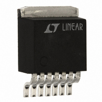
LT1506CR-3.3 Linear Technology, LT1506CR-3.3 Datasheet - Page 17

LT1506CR-3.3
Manufacturer Part Number
LT1506CR-3.3
Description
IC SW REG STEP-DOWN 500KHZ 7-DD
Manufacturer
Linear Technology
Type
Step-Down (Buck)r
Datasheet
1.LT1506CS8-3.3PBF.pdf
(24 pages)
Specifications of LT1506CR-3.3
Internal Switch(s)
Yes
Synchronous Rectifier
No
Number Of Outputs
1
Voltage - Output
3.3V
Current - Output
4.5A
Frequency - Switching
500kHz
Voltage - Input
4 ~ 15 V
Operating Temperature
0°C ~ 125°C
Mounting Type
Surface Mount
Package / Case
D²Pak, TO-263 (7 leads + tab)
Lead Free Status / RoHS Status
Contains lead / RoHS non-compliant
Power - Output
-
Available stocks
Company
Part Number
Manufacturer
Quantity
Price
Company:
Part Number:
LT1506CR-3.3
Manufacturer:
LT
Quantity:
5
Company:
Part Number:
LT1506CR-3.3
Manufacturer:
LT
Quantity:
5 510
Company:
Part Number:
LT1506CR-3.3
Manufacturer:
MOT
Quantity:
5 510
Part Number:
LT1506CR-3.3
Manufacturer:
LT/凌特
Quantity:
20 000
Company:
Part Number:
LT1506CR-3.3#TRPBF
Manufacturer:
TI
Quantity:
110
Part Number:
LT1506CR-3.3#TRPBF
Manufacturer:
LT/凌特
Quantity:
20 000
Company:
Part Number:
LT1506CR-3.3/IR
Manufacturer:
LT
Quantity:
500
APPLICATIONS
The term inside the radical has a maximum value of 0.5
when input voltage is twice output, and stays near 0.5 for
a relatively wide range of input voltages. It is common
practice therefore to simply use the worst-case value and
assume that RMS ripple current is one half of load current.
At maximum output current of 4.5A for the LT1506, the
input bypass capacitor should be rated at 2.25A ripple
current. Note however, that there are many secondary
considerations in choosing the final ripple current rating.
These include ambient temperature, average versus peak
load current, equipment operating schedule, and required
product lifetime. For more details, see Application Notes
19 and 46, and Design Note 95.
Input Capacitor Type
Some caution must be used when selecting the type of
capacitor used at the input to regulators. Aluminum
electrolytics are lowest cost, but are physically large to
achieve adequate ripple current rating, and size con-
straints (especially height), may preclude their use.
Ceramic capacitors are now available in larger values, and
their high ripple current and voltage rating make them
ideal for input bypassing. Cost is fairly high and footprint
may also be somewhat large. Solid tantalum capacitors
would be a good choice, except that they have a history of
occasional spectacular failures when they are subjected to
large current surges during power-up. The capacitors can
short and then burn with a brilliant white light and lots of
nasty smoke. This phenomenon occurs in only a small
percentage of units, but it has led some OEM companies
to forbid their use in high surge applications. The input
bypass capacitor of regulators can see these high surges
when a battery or high capacitance source is connected.
Several manufacturers have developed a line of solid
tantalum capacitors specially tested for surge capability
(AVX TPS series for instance, see Table 3), but even these
units may fail if the input voltage surge approaches the
maximum voltage rating of the capacitor. AVX recom-
mends derating capacitor voltage by 2:1 for high surge
applications.
Larger capacitors may be necessary when the input volt-
age is very close to the minimum specified on the data
sheet. Small voltage dips during switch on time are not
U
INFORMATION
U
W
U
normally a problem, but at very low input voltage they may
cause erratic operation because the input voltage drops
below the minimum specification. Problems can also
occur if the input-to-output voltage differential is near
minimum. The amplitude of these dips is normally a
function of capacitor ESR and ESL because the capacitive
reactance is small compared to these terms. ESR tends to
be the dominate term and is inversely related to physical
capacitor size within a given capacitor type.
SYNCHRONIZING (-SYNC Option for DD Package)
The SYNC pin, is used to synchronize the internal oscilla-
tor to an external signal. The SYNC input must pass from
a logic level low, through the maximum synchronization
threshold with a duty cycle between 10% and 90%. The
input can be driven directly from a logic level output. The
synchronizing range is equal to initial operating frequency
up to 1MHz. This means that minimum practical sync
frequency is equal to the worst-case high self-oscillating
frequency (560kHz), not the typical operating frequency of
500kHz. Caution should be used when synchronizing
above 700kHz because at higher sync frequencies the
amplitude of the internal slope compensation used to
prevent subharmonic switching is reduced. This type of
subharmonic switching only occurs at input voltages less
than twice output voltage. Higher inductor values will tend
to eliminate this problem. See Frequency Compensation
section for a discussion of an entirely different cause of
subharmonic switching before assuming that the cause is
insufficient slope compensation. Application Note 19 has
more details on the theory of slope compensation.
At power-up, when V
Figure 2, Q2), the sync function is disabled. This allows the
frequency foldback to operate in the shorted output con-
dition. During normal operation, switching frequency is
controlled by the internal oscillator until the FB pin reaches
1.5V, after which the SYNC pin becomes operational.
THERMAL CALCULATIONS
Power dissipation in the LT1506 chip comes from four
sources: switch DC loss, switch AC loss, boost circuit
current, and input quiescent current. The following
C
is being clamped by the FB pin (see
LT1506
17


