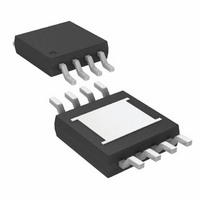
LT3505EMS8E#PBF Linear Technology, LT3505EMS8E#PBF Datasheet - Page 10

LT3505EMS8E#PBF
Manufacturer Part Number
LT3505EMS8E#PBF
Description
IC REG SW STP DWN 1.2A 8-MSOP
Manufacturer
Linear Technology
Type
Step-Down (Buck)r
Datasheet
1.LT3505EDDPBF.pdf
(24 pages)
Specifications of LT3505EMS8E#PBF
Internal Switch(s)
Yes
Synchronous Rectifier
No
Number Of Outputs
1
Voltage - Output
0.78 ~ 33.8 V
Current - Output
1.2A
Frequency - Switching
200kHz ~ 3MHz
Voltage - Input
3.6 ~ 36 V
Operating Temperature
-40°C ~ 85°C
Mounting Type
Surface Mount
Package / Case
8-MSOP Exposed Pad, 8-HMSOP, 8-eMSOP
Dc To Dc Converter Type
Step Down
Pin Count
8
Input Voltage
36V
Output Voltage
0.78 to 33.84V
Switching Freq
200 TO 3000KHz
Output Current
1.2A
Package Type
MSOP EP
Output Type
Adjustable
Switching Regulator
Yes
Line Regulation
0.007%/V(Typ)
Mounting
Surface Mount
Input Voltage (min)
3.6V
Operating Temp Range
-40C to 85C
Operating Temperature Classification
Industrial
Lead Free Status / RoHS Status
Lead free / RoHS Compliant
Power - Output
-
Lead Free Status / Rohs Status
Compliant
Available stocks
Company
Part Number
Manufacturer
Quantity
Price
LT3505
APPLICATIONS INFORMATION
10
AC COUPLED
AC COUPLED
200mV/DIV
AC COUPLED
200mV/DIV
200mV/DIV
0.5A/DIV
0.5A/DIV
20V/DIV
20V/DIV
0.5A/DIV
20V/DIV
V
V
V
OUT
V
V
SW
OUT
V
SW
OUT
I
I
SW
L
L
I
L
C
V
V
C
V
V
OUT
OUT
IN
C
V
V
OUT
OUT
IN
OUT
OUT
IN
= 30V
= 35V
= 40V
= 10 F
= 3V
= 10 F
= 3V
= 10µF
= 3V
I
L = 10 H
R
LOAD
T
I
L = 10 H
R
LOAD
I
L = 10µH
R
= 75.0k
T
LOAD
T
= 75.0k
= 75.0k
= 0.75A
Figure 3
Figure 1
Figure 2
= 0.75A
2 s/DIV
= 0.75A
2 s/DIV
2µs/DIV
3505 F01
3505 F02
3505 F03
Now the required on time has decreased below the
minimum on time of 130ns. Instead of the switch pulse
width becoming narrower to accommodate the lower duty
cycle requirement, the switch pulse width remains fi xed
at 130ns. In Figure 2 the inductor current ramps up to a
value exceeding the load current and the output ripple
increases to ~200mV. The part then remains off until the
output voltage dips below 100% of the programmed value
before it begins switching again.
For switching frequencies above 750kHz, the input voltage
must not exceed V
Foldback” section of the datasheet for a circuit solution
that provides safe operation above V
frequencies exceeding 750kHz. For switching frequencies
below 750kHz, operation above V
not damage the part as long as the output voltage stays
in regulation and the inductor does not saturate. Figure
3 shows the switching waveforms of a 750kHz applica-
tion when the input voltage is increased to its absolute
maximum rating of 40V.
As the input voltage increases, the inductor current ramp
rate increases, the number of skipped pulses increases
and the output voltage ripple increases. The part is robust
enough to survive prolonged operation under these condi-
tions as long as the programmed switching frequency is
less than 750kHz and the peak inductor current does not
exceed 2.2A. Inductor current saturation may further limit
performance in this operating regime.
Frequency Selection
The maximum frequency that the LT3505 can be pro-
grammed to is 3MHz. The minimum frequency that the
LT3505 can be programmed to is 200kHz. The switching
frequency is programmed by tying a 1% resistor from the R
pin to ground. Table 1 can be used to select the value of R
Minimum on-time and edge loss must be taken into consid-
eration when selecting the intended frequency of operation.
Higher switching frequency increases power dissipation
and lowers effi ciency.
IN(PS)
. See the “Input Voltage Frequency
IN(PS)
IN(PS)
is safe and will
at switching
3505fc
T
T
.


