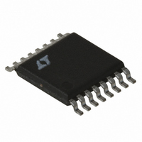
LT1766IFE#PBF Linear Technology, LT1766IFE#PBF Datasheet - Page 23

LT1766IFE#PBF
Manufacturer Part Number
LT1766IFE#PBF
Description
IC REG SW HV 1.5A 200KHZ 16TSSOP
Manufacturer
Linear Technology
Type
Step-Down (Buck)r
Datasheet
1.LT1766EGNPBF.pdf
(30 pages)
Specifications of LT1766IFE#PBF
Internal Switch(s)
Yes
Synchronous Rectifier
No
Number Of Outputs
1
Voltage - Output
1.2 ~ 54 V
Current - Output
1.5A
Frequency - Switching
200kHz
Voltage - Input
5.5 ~ 60 V
Operating Temperature
-40°C ~ 125°C
Mounting Type
Surface Mount
Package / Case
16-TSSOP Exposed Pad, 16-eTSSOP, 16-HTSSOP
Primary Input Voltage
60V
No. Of Outputs
1
Output Current
1.2A
No. Of Pins
16
Operating Temperature Range
-40°C To +125°C
Msl
MSL 1 - Unlimited
Supply Voltage Range
5.5V To 60V
Rohs Compliant
Yes
Dc To Dc Converter Type
Step Down
Pin Count
16
Input Voltage
60V
Output Voltage
1.2 to 54V
Switching Freq
216KHz
Package Type
TSSOP EP
Output Type
Adjustable
Switching Regulator
Yes
Mounting
Surface Mount
Input Voltage (min)
5.5V
Operating Temperature Classification
Automotive
Lead Free Status / RoHS Status
Lead free / RoHS Compliant
Power - Output
-
Lead Free Status / Rohs Status
Compliant
Available stocks
Company
Part Number
Manufacturer
Quantity
Price
APPLICATIONS INFORMATION
the V
cycle-skipping or odd/even cycle behavior is exhibited.
In summary:
1. Be aware that the simultaneous requirements of high
2. The simultaneous requirements of high V
FREQUENCY COMPENSATION
Before starting on the theoretical analysis of frequency
response, the following should be remembered—the
worse the board layout, the more diffi cult the circuit will
be to stabilize. This is true of almost all high frequency
analog circuits, read the Layout Considerations section
fi rst. Common layout errors that appear as stability prob-
lems are distant placement of input decoupling capacitor
and/or catch diode, and connecting the V
to a ground track carrying signifi cant switch current. In
addition, the theoretical analysis considers only fi rst order
non-ideal component behavior. For these reasons, it is
important that a fi nal stability check is made with produc-
tion layout and components.
The LT1766 uses current mode control. This alleviates
many of the phase shift problems associated with the
inductor. The basic regulator loop is shown in Figure 10.
The LT1766 can be considered as two g
amplifi er and the power stage.
Figure 11 shows the overall loop response. At the V
pin, the frequency compensation components used are:
R
capacitor used is a 100μF , 10V tantalum capacitor with
typical ESR of 100mΩ.
The ESR of the tantalum output capacitor provides a use-
ful zero in the loop frequency response for maintaining
C
V
practice due to internal dissipation. The Thermal Con-
siderations section offers a basis to estimate internal
power. In questionable cases a prototype supply should
be built and exercised to verify acceptable operation.
high f
switch on-time. Cycle skipping and/or odd/even cycle
behavior will result although correct output voltage is
usually maintained.
= 2.2k, C
IN
C
, high I
control voltage to the point where some sort of
OSC
can result in an unacceptably short minimum
OUT
C
= 0.022μF and C
and high f
OSC
may not be achievable in
F
= 220pF . The output
m
blocks, the error
C
IN
compensation
, low V
OUT
and
C
stability. This ESR, however, contributes signifi cantly to
the ripple voltage at the output (see Output Ripple Volt-
age in the Applications Section). It is possible to reduce
capacitor size and output ripple voltage by replacing the
tantalum output capacitor with a ceramic output capaci-
tor because of its very low ESR. The zero provided by the
tantalum output capacitor must now be reinserted back
into the loop. Alternatively there may be cases where,
even with the tantalum output capacitor, an additional
zero is required in the loop to increase phase margin for
improved transient response.
A zero can be added into the loop by placing a resistor,
R
tor, C
and the FB pin.
LT1766
C,
GND
CURRENT MODE
POWER STAGE
at the V
g
m
C
= 2mho
or by placing a capacitor, C
V
R
C
C
C
C
200k
R
O
C
Figure 10. Model for Loop Response
pin in series with the compensation capaci-
2000μmho
–20
–40
Figure 11. Overall Loop Response
80
60
40
20
g
C
0
AMPLIFIER
m
F
10
ERROR
=
V
V
I
C
PHASE
LOAD
IN
OUT
OUT
–
+
= 42V
= 5V
= 100μF, 10V, 0.1Ω
= 500mA
100
1.22V
V
LT1766/LT1766-5
GAIN
SW
FB
FREQUENCY (Hz)
1k
C
FB
10k
R
C
C
FB
R
C
F
R1
R2
C
LOAD
= 220pF
= 2.2k
= 22nF
, between the output
100k
1766 F10
1766 F11
+
1M
TANTALUM
ESR
C1
180
150
120
90
60
30
0
OUTPUT
23
CERAMIC
1766fc
ESL
C1


