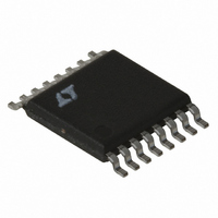
LT1765EFE-3.3 Linear Technology, LT1765EFE-3.3 Datasheet - Page 15

LT1765EFE-3.3
Manufacturer Part Number
LT1765EFE-3.3
Description
IC REG SW STEPDOWN 3A 16-TSSOP
Manufacturer
Linear Technology
Type
Step-Down (Buck)r
Datasheet
1.LT1765ES8PBF.pdf
(20 pages)
Specifications of LT1765EFE-3.3
Internal Switch(s)
Yes
Synchronous Rectifier
No
Number Of Outputs
1
Voltage - Output
3.3V
Current - Output
3A
Frequency - Switching
1.25MHz
Voltage - Input
3 ~ 25 V
Operating Temperature
-40°C ~ 125°C
Mounting Type
Surface Mount
Package / Case
16-TSSOP Exposed Pad, 16-eTSSOP, 16-HTSSOP
Lead Free Status / RoHS Status
Contains lead / RoHS non-compliant
Power - Output
-
Available stocks
Company
Part Number
Manufacturer
Quantity
Price
Part Number:
LT1765EFE-3.3
Manufacturer:
LINEAR/凌特
Quantity:
20 000
Company:
Part Number:
LT1765EFE-3.3#PBF
Manufacturer:
LT
Quantity:
7 000
Company:
Part Number:
LT1765EFE-3.3#TRPBF
Manufacturer:
LT
Quantity:
7 000
Part Number:
LT1765EFE-3.3#TRPBF
Manufacturer:
LINEAR/凌特
Quantity:
20 000
APPLICATIONS INFORMATION
Using the values shown in Figure 10,
The ramp is linear and rise times in the order of 100ms are
possible. Since the circuit is voltage controlled, the ramp
rate is unaffected by load characteristics and maximum
output current is unchanged. Variants of this circuit can
be used for sequencing multiple regulator outputs.
INPUT
2.2μF
12V
RiseTime
RiseTime
C3
Figure 10. Buck Converter with Adjustable Soft Start
+
=
V
SHDN
=
IN
SYNC
( )(
R
(
47 10 15 10
LT1765-5
4
330pF
BOOST
GND V
•
C
C
C
(
SS
V
REMOVABLE
V
BE
3
0.18μF
C
SW
)(
FB
)( •
)
0 7
V
INPUT
C2
.
OUT
Q1
)
D1
–
MBRS330T3*
Figure 9. Dual Source Supply with 6μA Reverse Leakage
CMDSH-3
9
83k
28.5k
* ONLY REQUIRED IF ADDITIONAL LOADS ON THE INPUT CAN SINK >10mA
5μH
)( )
R4
47k
L1
100μF
D2
5
R3
2k
C1
D1: B220A
Q1: 2N3904
=
15nF
C
SS
5
ms
2.2μF
V
SHDN
IN
SYNC
1765 F10
OUTPUT
5V
2.5A
LT1765-3.3
BOOST
GND
V
C
V
SW
0.18μF
FB
2.2nF
Dual Output Converter
The circuit in Figure 11 generates both positive and negative
5V outputs with a single piece of magnetics. The two induc-
tors shown are actually just two windings on a standard
B H Electronics inductor. The topology for the 5V output
is a standard buck converter. The –5V topology would be
a simple fl yback winding coupled to the buck converter
if C4 were not present. C4 creates a SEPIC (single-ended
primary inductance converter) topology which improves
regulation and reduces ripple current in L1. Without C4,
the voltage swing on L1B compared to L1A would vary
due to relative loading and coupling losses. C4 provides a
low impedance path to maintain an equal voltage swing in
L1B, improving regulation. In a fl yback converter, during
switch on time, all the converter’s energy is stored in L1A
only, since no current fl ows in L1B. At switch off, energy
is transferred by magnetic coupling into L1B, powering
the –5V rail. C4 pulls L1B positive during switch on time,
causing current to fl ow, and energy to build in L1B and
C4. At switch off, the energy stored in both L1B and C4
supply the –5V rail. This reduces the current in L1A and
changes L1B current waveform from square to triangular.
For details on this circuit, including maximum output cur-
rents, see Design Note 100
LT1765/LT1765-1.8/LT1765-2.5/
B220A
CMDSH-3
5μH
3.3V, 2A
4.7μF
LT1765-3.3/LT1765-5
ALTERNATE
1765 F09
SUPPLY
15
1765fd


