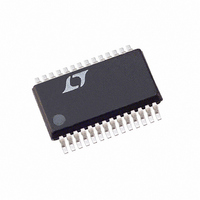
LTC3729EG Linear Technology, LTC3729EG Datasheet - Page 17

LTC3729EG
Manufacturer Part Number
LTC3729EG
Description
IC SW REG SYNC STEP-DOWN 28-SSOP
Manufacturer
Linear Technology
Series
PolyPhase®r
Type
Step-Down (Buck)r
Datasheet
1.LTC3729EGPBF.pdf
(30 pages)
Specifications of LTC3729EG
Internal Switch(s)
No
Synchronous Rectifier
Yes
Number Of Outputs
1
Voltage - Output
0.8 ~ 5 V
Current - Output
5A
Frequency - Switching
1.1MHz
Voltage - Input
4 ~ 36 V
Operating Temperature
-40°C ~ 85°C
Mounting Type
Surface Mount
Package / Case
28-SSOP
Lead Free Status / RoHS Status
Contains lead / RoHS non-compliant
Power - Output
-
Available stocks
Company
Part Number
Manufacturer
Quantity
Price
Part Number:
LTC3729EG#PBF
Manufacturer:
LINEAR/凌特
Quantity:
20 000
Company:
Part Number:
LTC3729EGN
Manufacturer:
PHILIPS
Quantity:
15
APPLICATIONS INFORMATION
gate‑source of the desired MOSFET. This enhances the
MOSFET and turns on the topside switch. The switch node
voltage, SW, rises to V
V
30 to 100 times that of the total input capacitance of the
topside MOSFET(s). The reverse breakdown of D
be greater than V
The final arbiter when defining the best gate drive amplitude
level will be the input supply current. If a change is made
that decreases input current, the efficiency has improved.
If the input current does not change then the efficiency
has not changed either.
Differential Amplifier/Output Voltage
The LTC3729 has a true remote voltage sense capablity.
The sensing connections should be returned from the load
back to the differential amplifier’s inputs through a common,
tightly coupled pair of PC traces. The differential amplifier
rejects common mode signals capacitively or inductively
radiated into the feedback PC traces as well as ground
loop disturbances. The differential amplifier output signal
is divided down and compared with the internal precision
0.8V voltage reference by the error amplifier.
The differential amplifier utilizes a set of internal preci‑
sion resistors to enable precision instrumentation‑type
measurement of the output voltage. The output is an NPN
emitter follower without any internal pull‑down current.
A DC resistive load to ground is required in order to sink
INTVCC
Figure 5a. Secondary Output Loop and EXTV
OPTIONAL EXTV
5V < V
EXTV
. The value of the boost capacitor C
CC
SEC
LTC3729
< 7V
CC
PGND
IN(MAX)
CONNECTION
SW1
BG1
TG1
V
C
IN
IN
+
IN
N-CH
N-CH
and the BOOST pin rises to V
.
V
1N4148
IN
T1
6.8V
R
SENSE
CC
B
V
Connection
SEC
needs to be
+
+
3729 F05a
B
1mF
C
V
OUT
OUT
must
IN
+
current. The output voltage is set by an external resistive
divider according to the following formula:
where R1 and R2 are defined in the Functional Diagram.
Soft-Start/Run Function
The RUN/SS pin provides three functions: 1) Run/Shut‑
down, 2) soft‑start and 3) a defeatable short‑circuit latchoff
timer. Soft‑start reduces the input power sources’ surge
currents by gradually increasing the controller’s current
limit I
treme load transients from tripping the overcurrent latch.
A small pull‑up current (>5µA) supplied to the RUN/SS
pin will prevent the overcurrent latch from operating.
The following explanation describes how the functions
operate.
An internal 1.2µA current source charges up the C
capacitor. When the voltage on RUN/SS reaches 1.5V, the
controller is permitted to start operating. As the voltage on
RUN/SS increases from 1.5V to 3.0V, the internal current
limit is increased from 25mV/R
The output current limit ramps up slowly, taking an ad‑
ditional 1.4µs/µF to reach full current. The output current
thus ramps up slowly, reducing the starting surge current
required from the input power supply. If RUN/SS has been
V
OUT
EXTV
TH(MAX)
Figure 5b. Capacitive Charge Pump for EXTV
CC
= 0.8V 1+
LTC3729
. The latchoff timer prevents very short, ex‑
PGND
SW1
BG1
TG1
C
V
IN
IN
R2
R1
+
N-CH
N-CH
BAT85
V
IN
L1
SENSE
VN2222LL
R
SENSE
to 75mV/R
LTC3729
0.22µF
+
+
CC
3729 F05b
17
BAT85
BAT85
1µF
C
V
SENSE
OUT
OUT
3729fb
SS
.


