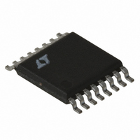
LT3434IFE Linear Technology, LT3434IFE Datasheet - Page 22

LT3434IFE
Manufacturer Part Number
LT3434IFE
Description
IC REG SW BUCK 3A 200KHZ 16TSSOP
Manufacturer
Linear Technology
Type
Step-Down (Buck)r
Datasheet
1.LT3434EFEPBF.pdf
(24 pages)
Specifications of LT3434IFE
Internal Switch(s)
Yes
Synchronous Rectifier
No
Number Of Outputs
1
Voltage - Output
1.25 ~ 54 V
Current - Output
3A
Frequency - Switching
200kHz
Voltage - Input
3.3 ~ 60 V
Operating Temperature
-40°C ~ 125°C
Mounting Type
Surface Mount
Package / Case
16-TSSOP Exposed Pad, 16-eTSSOP, 16-HTSSOP
Lead Free Status / RoHS Status
Contains lead / RoHS non-compliant
Power - Output
-
Available stocks
Company
Part Number
Manufacturer
Quantity
Price
Part Number:
LT3434IFE
Manufacturer:
LINEAR/凌特
Quantity:
20 000
Part Number:
LT3434IFE#PBF
Manufacturer:
LT凌特厂
Quantity:
20 000
Part Number:
LT3434IFE#TRPBF
Manufacturer:
LINEAR/凌特
Quantity:
20 000
LT3434
APPLICATIO S I FOR ATIO
catch diode and connecting the V
ground track carrying significant switch current. In addi-
tion the theoretical analysis considers only first order non-
ideal component behavior. For these reasons, it is important
that a final stability check is made with production layout
and components.
The LT3434 uses current mode control. This alleviates
many of the phase shift problems associated with the
inductor. The basic regulator loop is shown in Figure 12.
The LT3434 can be considered as two g
amplifier and the power stage.
Figure 13 shows the overall loop response with a 470pF V
capacitor and a typical 100µF tantalum output capacitor.
The response is set by the following terms:
The pole set by C
Unity gain frequency is set by C
Powerstage: DC gain is set by g
Pole set by C
Unity gain set by C
Tantalum output capacitor zero is set by C
ESR
The zero produced by the ESR of the tantalum output
capacitor is very useful in maintaining stability. If the ESR
of the output capacitor is low or better transient response
is required, a zero can be added to the loop using a resistor
(R
22
C
Error amplifier: DC gain is set by g
EA Gain = 650µ • 1.5M = 975
EA Pole = 1/(2π • 1.5M • 470pF) = 226Hz
EA Unity Gain Frequency = 650µF/(2π • 470pF)
PS DC Gain = 6 • 10 = 60
PS Pole = 1/(2π • 100µF • 10) = 159Hz
PS Unity Gain Freq = 6/(2π • 100µF) = 94kHz.
Output Capacitor Zero = 1/(2π • 100µF • 0.1) = 15.9kHz
) in series with the compensation capacitor (C
OUT
F
and R
and R
OUT
U
Ω
L
and g
:
L
U
:
= 220kHz
m
:
m
F
and g
and R
W
C
compensation to a
m
m
m
and R
L
blocks, the error
:
(assume 10Ω):
OUT
O
U
:
and C
C
). As
OUT
C
the value of R
generally improve but two effects limit its value. First, the
combination of output capacitor ESR and a large R
stop loop gain rolling off altogether. Second, if the loop
gain is not rolled off sufficiently at the switching frequency
output ripple will perturb the V
unstable duty cycle switching similar to subharmonic
oscillation. This may not be apparent at the output. Small-
signal analysis will not show this since a continuous time
system is assumed.
When checking loop stability the circuit should be oper-
ated over the application’s full voltage, current and tem-
perature range. Any transient loads should be applied and
the output voltage monitored for a well-damped behavior.
C
C
R
C
C
F
11
–40
–80
100
LT3434
80
40
0
V
CURRENT MODE
Figure 13. Model for Loop Response
C
POWER STAGE
10
Figure 14. Overall Loop Response
g
m
C
= 6
is increased, transient response will
100
Ω
g
1.5M
m
= 650µ
FREQUENCY (Hz)
1k
ERROR
AMP
Ω
–
+
V
C
C
R
C
I
10k
LOAD
OUT
OUT
F
C
C
= 470pF
= 10k
= 4700pF
C
= 3.3V
= 100µF, 0.1Ω
= 1A
pin enough to cause
1.25V
SW
SW
100k
FB
12
5
2
R1
R2
3434 F14
1M
3434 F13
180
160
120
80
40
0
C
FB
ESR
C
C
OUTPUT
OUT
may
3434fb


