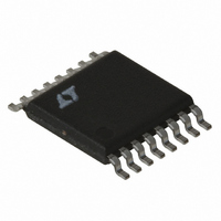
LT3434IFE#PBF Linear Technology, LT3434IFE#PBF Datasheet - Page 21

LT3434IFE#PBF
Manufacturer Part Number
LT3434IFE#PBF
Description
IC REG SW BUCK 3A 200KHZ 16TSSOP
Manufacturer
Linear Technology
Type
Step-Down (Buck)r
Datasheet
1.LT3434EFEPBF.pdf
(24 pages)
Specifications of LT3434IFE#PBF
Internal Switch(s)
Yes
Synchronous Rectifier
No
Number Of Outputs
1
Voltage - Output
1.25 ~ 54 V
Current - Output
3A
Frequency - Switching
200kHz
Voltage - Input
3.3 ~ 60 V
Operating Temperature
-40°C ~ 125°C
Mounting Type
Surface Mount
Package / Case
16-TSSOP Exposed Pad, 16-eTSSOP, 16-HTSSOP
Primary Input Voltage
60V
No. Of Outputs
1
Output Voltage
54V
Output Current
6.5A
No. Of Pins
16
Operating Temperature Range
-40°C To +125°C
Msl
MSL 1 - Unlimited
Rohs Compliant
Yes
Lead Free Status / RoHS Status
Lead free / RoHS Compliant
Power - Output
-
Available stocks
Company
Part Number
Manufacturer
Quantity
Price
APPLICATIO S I FOR ATIO
Example: with V
Total power dissipation is:
Thermal resistance for the LT3434 package is influenced
by the presence of internal or backside planes. With a full
plane under the FE16 package, thermal resistance will be
about 45°C/W. No plane will increase resistance to about
150°C/W. To calculate die temperature, use the proper
thermal resistance number for the desired package and
add in worst-case ambient temperature:
With the FE16 package (Q
temperature of 70°C:
Input Voltage vs Operating Frequency Considerations
The absolute maximum input supply voltage for the LT3434
is specified at 60V. This is based solely on internal semi-
conductor junction breakdown effects. Due to internal
power dissipation the actual maximum V
particular application may be less than this.
A detailed theoretical basis for estimating internal power
loss is given in the section Thermal Considerations. Note
that AC switching loss is proportional to both operating
frequency and output current. The majority of AC switch-
ing loss is also proportional to the square of input voltage.
For example, while the combination of V
5V at 2A and f
simultaneously raising V
not possible. Nevertheless, input voltage transients up to
60V can usually be accommodated, assuming the result-
P
T
T
P
P
P
0 08 0 62 0 7
BOOST
Q
J
J
SW
TOT
.
= T
= 70 + 45(0.84) = 108°C
= =
=
+
40 0 0026
= 0.7 + 0.03 + 0.109 = 0.84
A
(
=
0 15 2
(
.
+ Q
.
( )
.
5
=
JA
)( ) ( )
40
2
OSC
IN
40
(
(P
.
2 40
)
= 40V, V
/
2
TOT
+
U
= 200kHz may be easily achievable,
5
5 0 001
)
(
)
=
+
.
0 03
IN
(
U
77
.
OUT
JA
to 60V and f
e
)
=
–
= 45°C/W) at an ambient
= 5V and I
9 1 2 2 40 200
0 109
.
)
( )
W
/
( )( )
OSC
IN
IN
OUT
achievable in a
= 40V, V
to 700kHz is
= 2A:
(
U
e
OUT
3 3
)
=
ing increase in internal dissipation is of insufficient time
duration to raise die temperature significantly.
A second consideration is controllability. A potential limi-
tation occurs with a high step-down ratio of V
as this requires a correspondingly narrow minimum switch
on time. An approximate expression for this (assuming
continuous mode operation) is given as follows:
where:
A potential controllability problem arises if the LT3434 is
called upon to produce an on time shorter than its typical
value of 250ns. Feedback loop action will lower then
reduce the V
of cycle-skipping or Burst Mode behavior is exhibited.
In summary:
1. Be aware that the simultaneous requirements of high
2. The simultaneous requirements of high V
FREQUENCY COMPENSATION
Before starting on the theoretical analysis of frequency
response the following should be remembered—the worse
the board layout, the more difficult the circuit will be to
stabilize. This is true of almost all high frequency analog
circuits. Read the Layout Considerations section first.
Common layout errors that appear as stability problems
are distant placement of input decoupling capacitor and/or
t
V
V
V
f
V
practice due to internal dissipation. The Thermal Con-
siderations section offers a basis to estimate internal
power. In questionable cases a prototype supply should
be built and exercised to verify acceptable operation.
and high f
minimum switch on time. Cycle skipping and/or Burst
Mode behavior will result although correct output volt-
age is usually maintained.
ON(MIN)
OSC
IN
OUT
F
IN
= Schottky diode forward drop
, high I
= input voltage
= switching frequency
= output voltage
= V
C
OUT
control voltage to the point where some sort
OSC
OUT
and high f
can result in an unacceptably short
+ V
F
/V
IN
(f
OSC
OSC
may not be achievable in
)
LT3434
IN
IN
, low V
to V
21
OUT
3434fb
OUT
,


