IP1201TR International Rectifier, IP1201TR Datasheet - Page 10
IP1201TR
Manufacturer Part Number
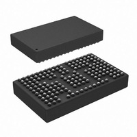
IP1201TR
Description
DUAL OUTPUT 2PH PWR BLOCK 198BGA
Manufacturer
International Rectifier
Series
iPOWIR™r
Type
Step-Down (Buck)r
Datasheet
1.IP1201TR.pdf
(29 pages)
Specifications of IP1201TR
Internal Switch(s)
Yes
Synchronous Rectifier
Yes
Number Of Outputs
2
Voltage - Output
0.8 ~ 3.3 V
Current - Output
30A
Frequency - Switching
200kHz ~ 400kHz
Voltage - Input
3.14 ~ 5.5 V
Operating Temperature
-40°C ~ 125°C
Mounting Type
Surface Mount
Package / Case
198-BGA (159 bumps)
Power - Output
6.7W
Package
BGA - 15.5 x 9.25
Circuit
Single Output or Dual Ch
Iout (a)
30
Switch Freq (khz)
200 - 400
Input Range (v)
3.14 - 5.5
Output Range (v)
0.9 - 3.3
Ocp Otp Uvlo Pre-bias Soft Start And
OVP + OCP + OTP and Soft Start
Pbf
PbF Option Available
For Use With
IRDCIP1201-A - BUCK CONV REF DESIGN KIT IP1201
Lead Free Status / RoHS Status
Contains lead / RoHS non-compliant
Available stocks
Company
Part Number
Manufacturer
Quantity
Price
Company:

Part Number:
IP1201TR
Manufacturer:
International Rectifier
Quantity:
10 000
Part Number:
IP1201TR
Manufacturer:
IR
Quantity:
20 000
Company:
Part Number:
IP1201TRPBF
Manufacturer:
IR
Quantity:
3 000
Company:
Part Number:
IP1201TRPBF
Manufacturer:
MICROCHIP
Quantity:
1 176
Company:
Part Number:
IP1201TRPBF
Manufacturer:
International Rectifier
Quantity:
10 000


iP1201
10
Pin Name
ENABLE
HICCUP
PGOOD
VSW1
VSW2
PGND
VP-ref
SYNC
FB1s
FB2s
CC1
CC2
SS1
SS2
FB1
FB2
Vref
NC
V
A*
B*
R
IN
T
E15 E16 F3 F4 F5 F6 F9 F10 F13 F14 F15 F16 G4 G5 G6
C10 C12 C13 D6 D7 D9 D10 D12 D13 D14 E3 E4 E8 E11
A6 A7 A9 A10 A12 A13 B6 B7 B9 B10 B12 B13 C6 C7 C9
D1 D2 D3 E1 E2 F1 F2 G1 G2 G3 H1 H2 H3 J1 J2 J3 K1
G9 G10 G13 G14 G15 H4 H5 H9 H10 H14 H15 J4 J5 J9
A1 A2 A3 A4 A5 A14 A15 A16 A17 A18 B1 B2 B3 B4 B5
D16 D17 D18 E17 E18 F17 F18 G16 G17 G18 H16 H17
B14 B15 B16 B17 B18 C1 C2 C3 C4 C5 C14 C15 C16
J10 J14 J15 K3 K16 L3 L5 L14 L16
H18 J16 J17 J18 K17 K18 L17 L18
Ball Designator
C17 C18
K2 L1 L2
L12 L13
G8 J13
A8 B8
L6 L7
G11
H13
H11
K13
L10
L11
J11
H8
H6
K6
J6
J8
L9
L8
Table 1: Pin Description
Logic level pin. Pulled high enables hiccup mode of operation. Pulled
low, turns both outputs ON. Should be pulled high to disable outputs.
output configuration. Refer to function description section on how to
Power Good pin, needs external pull-up resistor. If not used pin can
Amplifier 1 reference Voltage. Connect a 100pf cap from this pin to
Switching frequency setting pin. For R
Single pin for both outputs. Commands outputs ON or OFF. Pulled
External Clock synchronization pin. Set free running frequency to
80% of the SYNC frequency. When not in use leave pin floating.
Internally generated voltage. Connect to pin B when Vin < 3.5V.
Internally generated voltage. Connect to pin A when Vin < 3.5V.
Leave floating for input voltages >3.5V. Externally, add a 2.2µF
Leave floating for input voltages >3.5V. Externally, add a 2.2µF
Amplifier 2 reference voltage. Connect to Vref for independent
Output of the first error amplifier, refer to Fig.1 block diagram
provides soft start. Pulled low disables output 1.
provides soft start. Pulled low disables output 2.
Soft start pin for output1. External capacitor
Soft start pin for output2. External capacitor
low enables overcurrent shutdown mode.
Unused pin. No electrical connection.
Output of the second error amplifier
Output 1 inductor connection node
Output 2 inductor connection node
Inverting input of error amplifier 1
Inverting input of error amplifier 2
connect for parallel configuration.
Input voltage connection node
Output 1 voltage sense pin
Output 2 voltage sense pin
vs Frequency curve.
Pin Description
be left floating.
Power Ground
capacitor
capacitor
PGND.
T
selection, refer to Fig.11 R
www.irf.com
T
Related parts for IP1201TR
Image
Part Number
Description
Manufacturer
Datasheet
Request
R

Part Number:
Description:
DUAL OUTPUT 2PH PWR BLOCK 198BGA
Manufacturer:
International Rectifier
Datasheet:

Part Number:
Description:
SCHOTTKY RECTIFIER
Manufacturer:
International Rectifier Corp.
Datasheet:
Part Number:
Description:
SCHOTTKY RECTIFIER
Manufacturer:
International Rectifier Corp.
Datasheet:
Part Number:
Description:
SCHOTTKY RECTIFIER
Manufacturer:
International Rectifier Corp.
Datasheet:
Part Number:
Description:
SCHOTTKY RECTIFIER
Manufacturer:
International Rectifier Corp.
Datasheet:
Part Number:
Description:
SCHOTTKY RECTIFIER
Manufacturer:
International Rectifier Corp.
Datasheet:
Part Number:
Description:
SCHOTTKY RECTIFIER
Manufacturer:
International Rectifier Corp.
Datasheet:
Part Number:
Description:
SCHOTTKY RECTIFIER
Manufacturer:
International Rectifier Corp.
Datasheet:
Part Number:
Description:
SCHOTTKY RECTIFIER
Manufacturer:
International Rectifier Corp.
Datasheet:
Part Number:
Description:
SCHOTTKY RECTIFIER
Manufacturer:
International Rectifier Corp.
Datasheet:
Part Number:
Description:
SCHOTTKY RECTIFIER
Manufacturer:
International Rectifier Corp.
Datasheet:
Part Number:
Description:
SCHOTTKY RECTIFIER
Manufacturer:
International Rectifier Corp.
Datasheet:
Part Number:
Description:
SCHOTTKY RECTIFIER
Manufacturer:
International Rectifier Corp.
Datasheet:
Part Number:
Description:
SCHOTTKY RECTIFIER
Manufacturer:
International Rectifier Corp.
Datasheet:
Part Number:
Description:
SCHOTTKY RECTIFIER
Manufacturer:
International Rectifier Corp.
Datasheet: