IP1202TR International Rectifier, IP1202TR Datasheet - Page 9
IP1202TR
Manufacturer Part Number
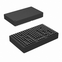
IP1202TR
Description
DUAL OUTPUT 2PH PWR BLOCK 198BGA
Manufacturer
International Rectifier
Series
iPOWIR™r
Type
Step-Down (Buck)r
Datasheet
1.IP1202.pdf
(29 pages)
Specifications of IP1202TR
Internal Switch(s)
Yes
Synchronous Rectifier
Yes
Number Of Outputs
2
Voltage - Output
0.8 ~ 5 V
Current - Output
30A
Frequency - Switching
200kHz ~ 400kHz
Voltage - Input
5.5 ~ 13.2 V
Operating Temperature
-40°C ~ 125°C
Mounting Type
Surface Mount
Package / Case
198-BGA (161 bumps)
Power - Output
7W
Input Voltage
13.2V
Output Current
15A
Output Voltage
5V
No. Of Outputs
2
No. Of Pins
198
Operating Temperature Range
-40°C To +125°C
Termination Type
SMD
Supply Voltage Min
5.5V
Rohs Compliant
No
Filter Terminals
SMD
Frequency
460kHz
Package
BGA - 15.5 x 9.25
Circuit
Single Output or Dual Ch
Iout (a)
30
Switch Freq (khz)
200 - 400
Input Range (v)
5.5 - 13.2
Output Range (v)
0.8 - 5.0
Ocp Otp Uvlo Pre-bias Soft Start And
OVP + OCP + OTP and Soft Start
Pbf
PbF Option Available
Lead Free Status / RoHS Status
Contains lead / RoHS non-compliant
Available stocks
Company
Part Number
Manufacturer
Quantity
Price
Company:

Part Number:
IP1202TR
Manufacturer:
EPSON
Quantity:
13 929
Company:
Part Number:
IP1202TR
Manufacturer:
International Rectifier
Quantity:
10 000
Company:
Part Number:
IP1202TRPBF
Manufacturer:
International Rectifier
Quantity:
10 000


www.irf.com
Pin Name
OCSET1
OCSET2
ENABLE
HICCUP
PGOOD
VSW1
VSW2
PGND
VP-ref
SYNC
FB1s
FB2s
CC1
CC2
SS1
SS2
FB1
FB2
Vref
V
R
IN
T
E15 E16 F3 F4 F5 F6 F8 F9 F10 F11 F13 F14 F15 F16 G3
A1 A2 A3 A4 A15 A16 A17 A18 B1 B2 B3 B4 B15 B16 B17
B13 B14 C5 C6 C7 C8 C9 C10 C11 C12 C13 C14 D5 D6
D1 D2 D3 E1 E2 F1 F2 G1 G2 H1 H2 J1 J2 K1 K2 L1 L2
D7 D8 D9 D10 D11 D12 D13 D14 E3 E4 E5 E6 E13 E14
D16 D17 D18 E17 E18 F17 F18 G17 G18 H17 H18 J17
A5 A6 A7 A9 A10 A12 A13 A14 B5 B6 B7 B10 B11 B12
G4 G6 G9 G10 G13 G15 G16 H4 H9 H10 H15 J4 J5 J9
J10 J14 J15 K4 K5 K14 K15 L3 L4 L5 L13 L14 L15 L16
B18 C1 C2 C3 C4 C15 C16 C17 C18
J18 K17 K18 L17 L18
Ball Designator
A8 B8
G11
H13
H11
J13
J11
L11
L10
G8
H6
H8
K6
J6
J8
L9
L8
L6
Table 1: Pin Description
Single pin for both outputs. Commands ouputs ON or OFF. Normally
Switching frequency setting pin. For R
Logic level pin. Pulled high enables hiccup mode of operation. Pulled
output configuration. Refer to application notes on how to connect to
Amplifier 1 reference Voltage. Connect a 100pF cap from this pin to
External Clock synchronization pin. Set free running frequency to
80% of the SYNC frequency. When not in use, leave pin floating
Soft start pin for output 1. External capacitor provides soft start.
Soft start pin for output 2. External capacitor provides soft start.
Amplifier 2 reference voltage. Connect to Vref for independent
parallel configuration or output voltage tracking configurations.
Power Good pin. Open collector, requires external pulll-up. If
low enables latched overcurrent shutdown mode.
Pulled High. Pulled low, turns both outputs ON.
Pulling soft start pin low will disable this output.
Pulling soft start pin low will disable this output.
function not needed, pin can be left floating
Overcurrent trip threshold pin for output 1
Overcurrent trip threshold pin for output 2
Output of the second error amplifier
Output 1 inductor connection pins
Output 2 inductor connection pins
Inverting input of error amplifier 1
Inverting input of error amplifier 2
Output of the first error amplifier
Output 1 overvoltage sense pin.
Output 2 overvoltage sense pin.
Input voltage connection pins
Power Ground pins
Pin Description
datasheet.
PGND.
T
selection, refer to Fig.9 of the
iP1202
9
Related parts for IP1202TR
Image
Part Number
Description
Manufacturer
Datasheet
Request
R

Part Number:
Description:
DUAL OUTPUT 2PH PWR BLOCK 198BGA
Manufacturer:
International Rectifier
Datasheet:

Part Number:
Description:
SCHOTTKY RECTIFIER
Manufacturer:
International Rectifier Corp.
Datasheet:
Part Number:
Description:
SCHOTTKY RECTIFIER
Manufacturer:
International Rectifier Corp.
Datasheet:
Part Number:
Description:
SCHOTTKY RECTIFIER
Manufacturer:
International Rectifier Corp.
Datasheet:
Part Number:
Description:
SCHOTTKY RECTIFIER
Manufacturer:
International Rectifier Corp.
Datasheet:
Part Number:
Description:
SCHOTTKY RECTIFIER
Manufacturer:
International Rectifier Corp.
Datasheet:
Part Number:
Description:
SCHOTTKY RECTIFIER
Manufacturer:
International Rectifier Corp.
Datasheet:
Part Number:
Description:
SCHOTTKY RECTIFIER
Manufacturer:
International Rectifier Corp.
Datasheet:
Part Number:
Description:
SCHOTTKY RECTIFIER
Manufacturer:
International Rectifier Corp.
Datasheet:
Part Number:
Description:
SCHOTTKY RECTIFIER
Manufacturer:
International Rectifier Corp.
Datasheet:
Part Number:
Description:
SCHOTTKY RECTIFIER
Manufacturer:
International Rectifier Corp.
Datasheet:
Part Number:
Description:
SCHOTTKY RECTIFIER
Manufacturer:
International Rectifier Corp.
Datasheet:
Part Number:
Description:
SCHOTTKY RECTIFIER
Manufacturer:
International Rectifier Corp.
Datasheet:
Part Number:
Description:
SCHOTTKY RECTIFIER
Manufacturer:
International Rectifier Corp.
Datasheet:
Part Number:
Description:
SCHOTTKY RECTIFIER
Manufacturer:
International Rectifier Corp.
Datasheet: