LM2574MX-3.3/NOPB National Semiconductor, LM2574MX-3.3/NOPB Datasheet
LM2574MX-3.3/NOPB
Specifications of LM2574MX-3.3/NOPB
*LM2574MX-3.3/NOPB
LM2574MX-3.3
Available stocks


Related parts for LM2574MX-3.3/NOPB


LM2574MX-3.3/NOPB Summary of contents
Page 1
... Typical Application (Fixed Output Voltage Versions) Note: Pin numbers are for 8-pin DIP package. Patent Pending SIMPLE SWITCHER ™ trademark of National Semiconductor Corporation © 1999 National Semiconductor Corporation DS011394 0.5A Step-Down Voltage Regulator ™ Features n 3.3V, 5V, 12V, 15V, and adjustable output versions n Adjustable version output voltage range, 1 ...
Page 2
Connection Diagrams 8-Lead DIP DS011394 internal connection, but should be soldered to PC board for best heat transfer. Top View Order Number LM2574-3.3HVN, LM2574HVN-5.0, LM2574HVN-12, LM2574HVN-15, LM2574HVN-ADJ, LM2574N-3.3, LM2574N-5.0, LM2574N-12, LM2574N-15 or LM2574N-ADJ See NS Package Number N08A ...
Page 3
... Absolute Maximum Ratings If Military/Aerospace specified devices are required, please contact the National Semiconductor Sales Office/ Distributors for availability and specifications. Maximum Supply Voltage LM2574 LM2574HV ON /OFF Pin Input Voltage Output Voltage to Ground (Steady State) Minimum ESD Rating (C = 100 pF 1 Storage Temperature Range LM2574-3 ...
Page 4
LM2574-12, LM2574HV-12 Electrical Characteristics Specifications with standard type face are for T ture Range. Symbol Parameter SYSTEM PARAMETERS (Note 3) Test Circuit Figure 2 = 25V Output Voltage V OUT IN V Output Voltage 15V OUT LM2574 V ...
Page 5
LM2574-ADJ, LM2574HV-ADJ Electrical Characteristics Specifications with standard type face are for T ture Range. Unless otherwise specified, V Symbol Parameter SYSTEM PARAMETERS (Note 3) Test Circuit Figure 2 V Feedback Voltage LM2574 V Programmed for 5V. ...
Page 6
All Output Voltage Versions Electrical Characteristics Specifications with standard type face are for T ture Range. Unless otherwise specified 30V for the 15V version. I and V IN LOAD Symbol Parameter ON /OFF CONTROL Test Circuit Figure 2 ...
Page 7
Typical Performance Characteristics Current Limit DS011394-30 Oscillator Frequency DS011394-33 Minimum Operating Voltage DS011394-36 (Circuit of Figure 2 ) (Continued) Supply Current DS011394-31 Switch Saturation Voltage DS011394-34 Supply Current vs Duty Cycle DS011394-37 7 Standby Quiescent Current DS011394-32 Efficiency DS011394-35 Feedback ...
Page 8
Typical Performance Characteristics Feedback Pin Current DS011394-39 Continuous Mode Switching Waveforms = 5V, 500 mA Load Current 330 µH V OUT Notes: A: Output Pin Voltage, 10V/div B: Inductor Current, 0.2 A/div C: Output Ripple Voltage, 20 mV/div, ...
Page 9
Block Diagram 3.3V 1.7k 5V 3.1k 12V 8.84k 15V 11.3k For Adj. Version R1 = Open Note: Pin numbers are for the 8-pin DIP package. FIGURE ...
Page 10
Test Circuit and Layout Guidelines C — 22 µF, 75V IN Aluminum Electrolytic C — 220 µF, 25V OUT Aluminum Electrolytic D1 — Schottky, 11DQ06 L1 — 330 µH, 52627 (for 5V in, 3.3V out, use 100 µH, RL-1284-100) R1 ...
Page 11
Test Circuit and Layout Guidelines (Continued) Inductor Pulse Eng. Renco Value (Note 1) (Note µH RL-1284-68-43 100 µH * RL-1284-100-43 150 µH 52625 RL-1284-150-43 220 µH 52626 RL-1284-220-43 330 µH 52627 RL-1284-330-43 470 µH 52628 RL-1284-470-43 680 ...
Page 12
LM2574 Series Buck Regulator Design Procedure PROCEDURE (Fixed Output Voltage Versions) Given: = Regulated Output Voltage (3.3V, 5V, 12V, or 15V) V OUT (Max) = Maximum Input Voltage V IN (Max) = Maximum Load Current I LOAD 1. Inductor Selection ...
Page 13
LM2574 Series Buck Regulator Design Procedure INDUCTOR VALUE SELECTION GUIDES (For Continuous Mode Operation) FIGURE 4. LM2574HV-3.3 Inductor Selection Guide FIGURE 5. LM2574HV-5.0 Inductor Selection Guide (Continued) DS011394-26 FIGURE 6. LM2574HV-12 Inductor Selection Guide DS011394-13 FIGURE 7. LM2574HV-15 Inductor Selection ...
Page 14
LM2574 Series Buck Regulator Design Procedure FIGURE 8. LM2574HV-ADJ Inductor Selection Guide PROCEDURE (Adjustable Output Voltage Versions) Given: = Regulated Output Voltage V OUT (Max) = Maximum Input Voltage V IN (Max) = Maximum Load Current I LOAD F = ...
Page 15
LM2574 Series Buck Regulator Design Procedure PROCEDURE (Adjustable Output Voltage Versions) 3. Output Capacitor Selection (C ) OUT A. The value of the output capacitor together with the inductor defines the dominate pole-pair of the switching regulator loop. For stable ...
Page 16
LM2574 Series Buck Regulator Design Procedure Application Hints INPUT CAPACITOR ( maintain stability, the regulator input pin must be by- passed with at least a 22 µF electrolytic capacitor. The ca- pacitor’s leads must be kept short, ...
Page 17
Application Hints (Continued) INDUCTOR RIPPLE CURRENT When the switcher is operating in the continuous mode, the inductor current waveform ranges from a triangular to a saw- tooth type of waveform (depending on the input voltage). For a given input voltage ...
Page 18
Application Hints (Continued) pacitor and the amplitude of the inductor ripple current ( I ). See the section on inductor ripple current in Applica- IND tion Hints. The lower capacitor values (100 µF- 330 µF) will allow typi- cally 50 ...
Page 19
Application Hints (Continued) The data sheet thermal resistance curves and the thermal model in Switchers Made Simple software (version 3.3) can estimate the maximum junction temperature based on operating conditions. ln addition, the junction temperature can be estimated in actual ...
Page 20
Additional Applications Note: Pin numbers are for 8-pin DIP package. FIGURE 12. Negative Boost Because of the boosting function of this type of regulator, the switch current is relatively high, especially at low input volt- ages. Output load current limitations ...
Page 21
Additional Applications (Continued) Note: Pin numbers are for 8-pin DIP package. FIGURE 16. 1.2V to 55V Adjustable 500 mA Power Supply with Low Output Ripple Definition of Terms BUCK REGULATOR A switching regulator topology in which a higher voltage is ...
Page 22
Definition of Terms (Continued) INDUCTOR SATURATION The condition which exists when an inductor cannot hold any more magnetic flux. When an inductor saturates, the induc- tor appears less inductive and the resistive component domi- nates. Inductor current is then limited ...
Page 23
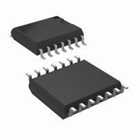
Physical Dimensions inches (millimeters) unless otherwise noted Order Number LM2574M-3.3, LM2574HVM-3.3, LM2574M-5.0, LM2574HVM-5.0, LM2574M-12, LM2574HVM-12, LM2574M-15, LM2574HVM-15, LM2574M-ADJ or LM2574HVM-ADJ 14-Lead Wide Surface Mount (WM) NS Package Number M14B 23 www.national.com ...
Page 24
... NATIONAL’S PRODUCTS ARE NOT AUTHORIZED FOR USE AS CRITICAL COMPONENTS IN LIFE SUPPORT DEVICES OR SYSTEMS WITHOUT THE EXPRESS WRITTEN APPROVAL OF THE PRESIDENT AND GENERAL COUNSEL OF NATIONAL SEMICONDUCTOR CORPORATION. As used herein: 1. Life support devices or systems are devices or systems which, (a) are intended for surgical implant ...