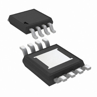
LM5085MY/NOPB National Semiconductor, LM5085MY/NOPB Datasheet - Page 3

LM5085MY/NOPB
Manufacturer Part Number
LM5085MY/NOPB
Description
IC BUCK ADJ 8MSOPEP
Manufacturer
National Semiconductor
Series
PowerWise®r
Type
Step-Down (Buck)r
Datasheet
1.LM5085MYENOPB.pdf
(22 pages)
Specifications of LM5085MY/NOPB
Design Resources
LM(2)5085 Quick Start Calculator
Internal Switch(s)
No
Synchronous Rectifier
No
Number Of Outputs
1
Voltage - Output
1.25 ~ 75 V
Frequency - Switching
Up to 1MHz
Voltage - Input
4.5 ~ 75 V
Operating Temperature
-40°C ~ 125°C
Mounting Type
Surface Mount
Package / Case
8-MSOP Exposed Pad, 8-HMSOP, 8-eMSOP
Lead Free Status / RoHS Status
Lead free / RoHS Compliant
Current - Output
-
Power - Output
-
Other names
LM5085MY
Available stocks
Company
Part Number
Manufacturer
Quantity
Price
Company:
Part Number:
LM5085MY/NOPB
Manufacturer:
TI
Quantity:
1 001
Part Number:
LM5085MY/NOPB
Manufacturer:
TI/德州仪器
Quantity:
20 000
No.
Pin
Pin Descriptions
1
2
3
4
5
6
7
8
PGATE Gate Driver Output
Name
ISEN
GND
VCC
ADJ
VIN
RT
FB
EP
Description
Current Limit Adjust
On-time control and shutdown
Voltage Feedback from the
regulated output
Circuit Ground
Current sense input for current
limit detection.
Output of the gate driver bias
regulator
Input supply voltage
Exposed Pad
Application Information
The current limit threshold is set by an external resistor from VIN to ADJ in
conjunction with the external sense resistor or the PFET’s R
An external resistor from VIN to RT sets the buck switch on-time and switching
frequency. Grounding this pin shuts down the controller.
Input to the regulation and over-voltage comparators. The regulation level is
1.25V.
Ground reference for all internal circuitry
Connect to the PFET drain when using R
PFET source and the sense resistor when using a current sense resistor.
Connect to the gate of the external PFET.
Output of the negative voltage regulator (relative to VIN) that biases the PFET
gate driver. A low ESR capacitor is required from VIN to VCC, located as close
as possible to the pins.
The operating input range is from 4.5V to 75V. A low ESR bypass capacitor must
be located as close as possible to the VIN and GND pins.
Exposed pad on the underside of the package (MSOP-8EP and LLP only). This
pad is to be soldered to the PC board ground plane to aid in heat dissipation.
3
DS(ON)
current sense. Connect to the
DS(ON)
.
www.national.com


